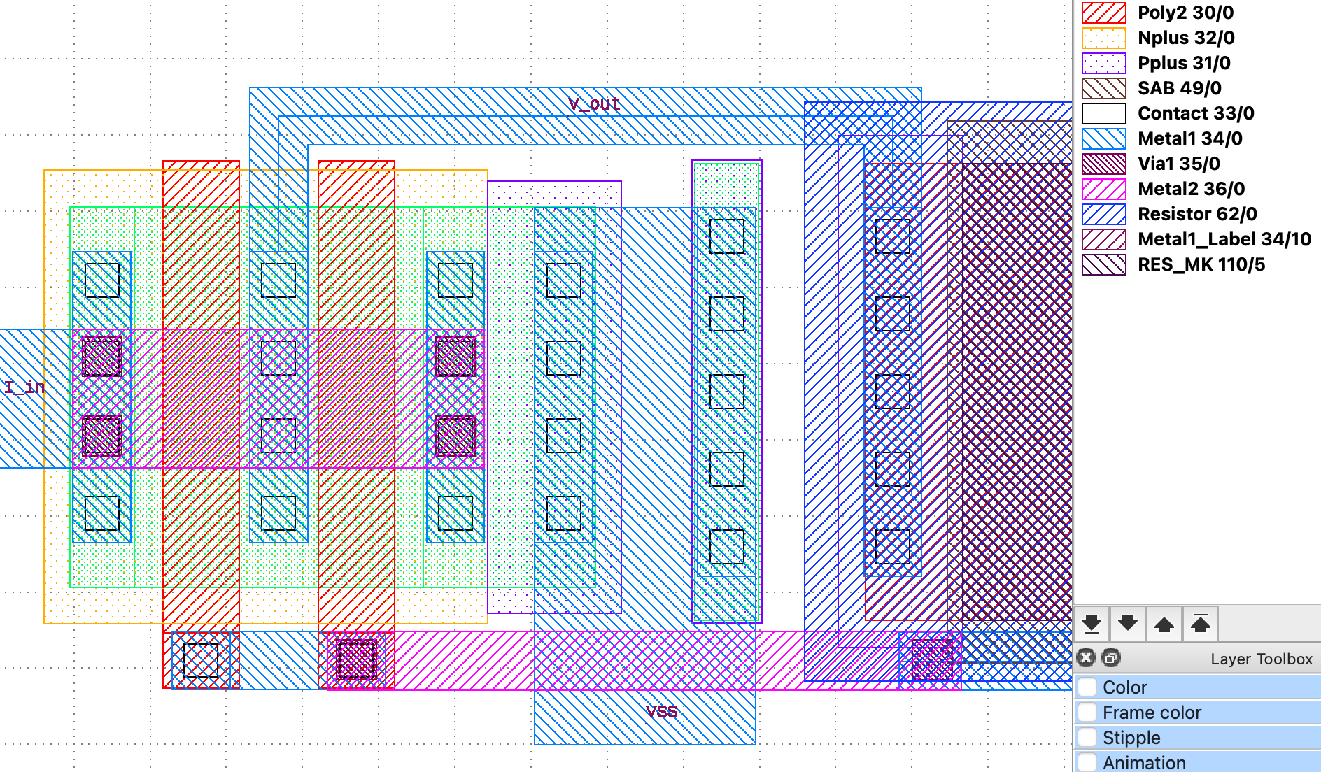
The gf180mcu process allows tap diffusion to abut mosfet source drain.
Thinking just about the doped silicon, this is a lateral parasitic diode - not extracted as a device and not connected.
However, I think gf180mcu adds a salicide step to the diffusion to reduce resistance. This effectively creates a low resistance layer over all diffusion (not blocked) irregardless of doping.
If this is true, then abutting tap and mosfet source/drain are shorted.
In the pdk used for chipathon 2026, the magic tech file extracts abutting tap and mosfet source/drain as shorted, but the klayout tech file does not.
Does wafer.space use a modified klayout rule that shorts the abutting diffusions?
@Leo Moser (mole99) (edited)




 1


 1