Hi all,
Our design passed the open-source KLayout DRC checks and wafer.space precheck (not the lastest version), but a commercial DRC run reported additional violations.
Some commercial checks appear to be absent from the open-source deck versions we used. In particular, we could not find an implementation of PAD.15, so passing the open-source checks does not appear to establish compliance with this guideline.
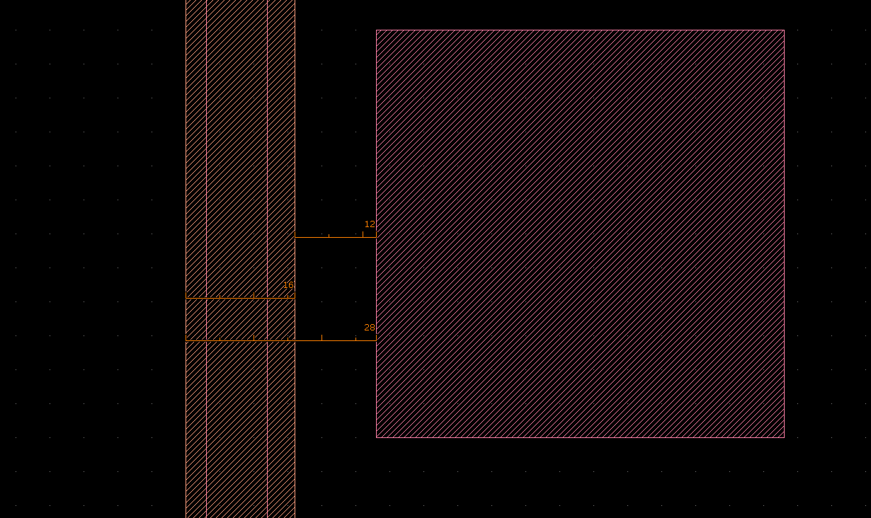
For example, the commercial run reported 87 PAD.15 results. The public GF180 bond-pad guidelines (https://gf180mcu-pdk.readthedocs.io/en/latest/physical_verification/design_manual/drm_09_2.html) specify a 30 µm minimum distance between the pad opening and the inner edge of GUARD_RING_MK.
At a representative location along the left die edge, the inner edge of GUARD_RING_MK is at x = 16 µm, and the nearest pad-opening edge is at x = 28 µm, giving a separation of 12 µm.
Our PAD_EDGE_SPACING is 26 µm, which is the default supplied by the GF180 PDK’s LibreLane I/O configuration in the version we use.
Could anyone clarify whether these additional commercial DRC violations must be corrected before submission, or whether applicable exceptions allow them to be accepted despite the commercial results?
Specifically, is this 12 µm PAD.15 spacing acceptable, or does it require a layout change?
Our design uses a 1×0.5 slot with COB, gf180mcuD, and gf180mcu_fd_io pads. The commercial run selected WEDGE bonding; the public PAD.15 table lists 30 µm for wedge, ball, and gold-bump options.
Thank you!
Hello @Edmund,
Similar as in your other question, the GF-MPW shuttles were previously taped out with the same configuration.
PAD.15 is a bond pad guideline, however it always depends on what your assembly house is capable of. You can adjust the spacing to the guard ring to comply with PAD.15 if you wish, but this means that your chip won't be compatible with the default CoB packaging offered by wafer.space.
You can also just keep it as it is in the default LibreLane template. Many designs on https://github.com/wafer-space/ws-run1 and https://github.com/wafer-space/ws-run2 use the same configuration.