Guild icon
wafer.space Community
ℹ️ - Information / ⁉️-questions / WLCSP ?
Between 2026-06-30 11:59 p.m. and 2026-08-01 12:00 a.m.

Avatar
Hello I own a small PnP business. We very reliably Pick-and-Place 300µm pitch BGA family part. Without much knowledge of the silicon making process. Would it be possible to create a 300µm grid of 100µm gold pads on the top metal layer; reflow some ready made balls on the top of the chip; And reflow it directly to the PCB ? (I guess add some epoxy at some point too) --- I don't particularly care for WLCSP or BGA, QFN is much easier to inspect, but WLCSP looks like a packaging method which doesn't require much equipement beyond a good 0402 or 0201 class pick and place machine. (edited)
12:12 a.m.
(Such pick and place cost start at 1k$ to 2k$ but they come with a steep learning curve to get such good results.) (edited)
Avatar
Hum if my search is to believed I would need an extra masked sputtering step to deposit gold on the top side of the IC.
12:21 a.m.
sounds highly automatable, I guess it would be much cheaper than wire bonding ?
Avatar
The chip itself has aluminium top metal and silicon nitride passivation. It is possible to expose only the bond pads from the passivation (there are options already prepared in the design rule checks). If you have an ability to bond that out through a flip-chip process, at a cost cheaper than the chips themselves, at these quantities you can see on the website (i.e., 1k chips for 4~10 $ each depending on if half or full slot and depending on whether early bird discount applies), please share.
12:23 a.m.
Notably, per my research, there are electroless zincate base plating methods available to build up a standard ENIG stackup or other such solderable surface on the aluminium, without needing high vacuum or any further lithography.
Avatar
Avatar
namibj
Notably, per my research, there are electroless zincate base plating methods available to build up a standard ENIG stackup or other such solderable surface on the aluminium, without needing high vacuum or any further lithography.
oohh
Avatar
I'll draw a few test pad-pairs of realistic proportions (but not the same proportions throughout) that target bonding via AnisotropicConductiveFilm to high-fidelity (mostly due to copper thickness though) COTS FPC (polyimide core, 0.33 oz copper either side, "solder mask" much less detailed than the copper features themselves, so fine pitch would have to be without solder mask bridges between pads), specifically the 2L FPC special offer at JLCPCB (for prototyping convenience, and as it's realistic). If you happen to have some plating/bumping targeted pad-pair geometries in mind, feel free to join/contribute/share.
12:29 a.m.
we haven't yet found an affordable performant (more than the ACF can offer, at least) option for flip-chip packaging at the quantities we're dealing with here, sadly, so therefore contributions would be well-received.
Avatar
Ok so I see 3 problems 1. readying the ICs for accepting the balls 2. applying balls, I don't have experience given commerce ICs come with balls I've seen plenty of electronics repair people doing this everyday with nearly 100% yield and artiasanal equipement (jigs and laser cut steel stencils), so we should be able to find that knowledge in the wild 3. soldering to a PCB, that I know how to do, there are lots of tricks, but basically you must have a flat PCB (ENIG), a good PCB footprint, and a well callibrated pnp, then you "just" place it correctly ~+-80µm in XY and it always work (/ I never had a failure yet)
Avatar
Avatar
namibj
I'll draw a few test pad-pairs of realistic proportions (but not the same proportions throughout) that target bonding via AnisotropicConductiveFilm to high-fidelity (mostly due to copper thickness though) COTS FPC (polyimide core, 0.33 oz copper either side, "solder mask" much less detailed than the copper features themselves, so fine pitch would have to be without solder mask bridges between pads), specifically the 2L FPC special offer at JLCPCB (for prototyping convenience, and as it's realistic). If you happen to have some plating/bumping targeted pad-pair geometries in mind, feel free to join/contribute/share.
I'm not sure I understand that, is your "roadmap" different ?
Avatar
(AFAIK, as long as this does not inhibit the wire bonding ability for those customers/slots who have planned to do that, it would be possible to do the electroless/plating build-up pre-dicing at wafer-scale, provided it's not a significant expense to treat the other dies; but aside from any thick gold options, I don't think any of the plating here would have reason to be too expensive to afford wasting it on the non-flip-chip dies just to get to plate the flip-chip-dies before the wafers get diced.)
👍 1
❤️ 1
Avatar
Avatar
Jorropo
Ok so I see 3 problems 1. readying the ICs for accepting the balls 2. applying balls, I don't have experience given commerce ICs come with balls I've seen plenty of electronics repair people doing this everyday with nearly 100% yield and artiasanal equipement (jigs and laser cut steel stencils), so we should be able to find that knowledge in the wild 3. soldering to a PCB, that I know how to do, there are lots of tricks, but basically you must have a flat PCB (ENIG), a good PCB footprint, and a well callibrated pnp, then you "just" place it correctly ~+-80µm in XY and it always work (/ I never had a failure yet)
Essentially the chip itself is bare aluminium LGA
Avatar
I would suspect that if we can do flip-chip no one would want wire bonding ¿ 😄
12:34 a.m.
(take that with a huge grain of salt I'm no where an expert here)
Avatar
Avatar
namibj
I'll draw a few test pad-pairs of realistic proportions (but not the same proportions throughout) that target bonding via AnisotropicConductiveFilm to high-fidelity (mostly due to copper thickness though) COTS FPC (polyimide core, 0.33 oz copper either side, "solder mask" much less detailed than the copper features themselves, so fine pitch would have to be without solder mask bridges between pads), specifically the 2L FPC special offer at JLCPCB (for prototyping convenience, and as it's realistic). If you happen to have some plating/bumping targeted pad-pair geometries in mind, feel free to join/contribute/share.
ok sorry what is that trying to test ? Afait you want to make a PCB that an analog for the top of the IC and try to develop a flipped die process on it ?
Avatar
If you have connections/access to plating that can turn that into something you can "just" solder, I believe appropriate stencil thickness should suffice to form a robust-to-manufacture gap between the die and the PCB? Because that's the main reason for the balls, right, vs. "just" using LGA?
Avatar
Avatar
namibj
If you have connections/access to plating that can turn that into something you can "just" solder, I believe appropriate stencil thickness should suffice to form a robust-to-manufacture gap between the die and the PCB? Because that's the main reason for the balls, right, vs. "just" using LGA?
I have zero LGA experience. If you get balls on an IC it's really easy to reflow* *assuming you've got high quality balls and they havn't been reflowed more than 2 times already and are full of oxides.
12:37 a.m.
Well I don't know the right word in english, but I and plenty of other peoples are making this happen every day like it's nothing.
Avatar
Avatar
Jorropo
ok sorry what is that trying to test ? Afait you want to make a PCB that an analog for the top of the IC and try to develop a flipped die process on it ?
ACF is the flip-chip/non-soldering bonding technology that's mainstream used to attach active-matrix displays and other such circuits on glass to more traditional printed circuits and also to directly attach driver ASIC dies to the display glass. It's low cost and doesn't necessarily need plating, but it's high resistance compared to soldering and only liked by the display industry because it's much easier to hot-press an epoxy carrier tape (the ACF matrix loaded with nickel balls that when compressed perform the anisotropic conductive aspect) for 10 seconds at 200C than to deal with flux and solder-melting temperatures when a TFT display's traces-on-glass are involved. I'm placing a few test pad pairs (likely one connected to GND and the other to VDD, or something; to ideally test that the adjacent pads don't short out to each other) on otherwise "spare" silicon area on the current tapeout (Run2), to hopefully qualify this flip-chip process for (limited) production use on the next run.
Avatar
Avatar
namibj
ACF is the flip-chip/non-soldering bonding technology that's mainstream used to attach active-matrix displays and other such circuits on glass to more traditional printed circuits and also to directly attach driver ASIC dies to the display glass. It's low cost and doesn't necessarily need plating, but it's high resistance compared to soldering and only liked by the display industry because it's much easier to hot-press an epoxy carrier tape (the ACF matrix loaded with nickel balls that when compressed perform the anisotropic conductive aspect) for 10 seconds at 200C than to deal with flux and solder-melting temperatures when a TFT display's traces-on-glass are involved. I'm placing a few test pad pairs (likely one connected to GND and the other to VDD, or something; to ideally test that the adjacent pads don't short out to each other) on otherwise "spare" silicon area on the current tapeout (Run2), to hopefully qualify this flip-chip process for (limited) production use on the next run.
how will you attach it to the IC ?
Avatar
Avatar
Jorropo
I have zero LGA experience. If you get balls on an IC it's really easy to reflow* *assuming you've got high quality balls and they havn't been reflowed more than 2 times already and are full of oxides.
We don't know where to affordably get balls onto the currently produced chips; though their aluminium is actually more a hindrance than the shape.
Avatar
I have found a TI resources about their ENIG on IC process
12:45 a.m.
I call it Z conductive tape but I guess that not the industry term 😄
Avatar
I'll be back later my dinner is getting cold 😉
Sparkles 1
Avatar
Avatar
namibj
I'll be back later my dinner is getting cold 😉
bonne appétit
Avatar
Avatar
Jorropo
I call it Z conductive tape but I guess that not the industry term 😄
this ACF style is afaik from a family of z-conductive tape stuff
12:49 a.m.
Also, you mentioned 300um pitch; we'd prefer to hit about 100~150 um pitch at least in an appriximately-QFN-style pad layout (i.e., single-row, all or at least multiple sides).
Avatar
100µm is tight
12:50 a.m.
on a good day (aka not heatwave) my placement deviation is like 25~50µm
12:50 a.m.
altho I have a cheap opensource pick and place
12:51 a.m.
if you've spent 10k$ or gave me 6 months to make and refine my own pnp we could probably make it happen
Avatar
the chips take about that long to finish anyways
Avatar
If you just wanted to place on a carrier, you could use some kind of micro manipulator with openpnp and a high resolution camera and optics and you should be able to place with single digit µm accuracy (the hardest thing is keeping everything square at all time, thermal dilation of 1m aluminium is so anoying) (edited)
Avatar
what to think of now is what geometry is still practical enough (both pad size and spacing between) to work; notably, accounting for whatever the plating process does
👍 1
Avatar
If my researches are to be believied, adding gold to the top of a wafer is a standard process. Is that something the fab would be able to offer ? (altho I guess it would do the whole wafer)
Avatar
yeah I'm planning for https://www.youtube.com/watch?v=MgQbPdiuUTw -based motion of the die and see-through optics through at least alignment holes in the copper of the 2L flex to line up with the die.
Sparkles 1
Avatar
Avatar
namibj
yeah I'm planning for https://www.youtube.com/watch?v=MgQbPdiuUTw -based motion of the die and see-through optics through at least alignment holes in the copper of the 2L flex to line up with the die.
Just so you know lots of the software work is accounting for the X Y and Z axis not being at perfect 90° of each other
12:56 a.m.
there are so many layers of self calibration and compensations
Avatar
I'm not aware of global foundries offering us plating options, sadly; at least not at these quantities we buy from them (for them it's literally "singular full MOQ" size; they do offer half-batches for very small quantities but the cost per chip is like +50% or even +80%, so it's not suitable for production orders). There should be some third party facilities offering such services, though.
Avatar
It looks like it's "just" applying chemicals baths to the top of the wafer. They could combine it with someone's else big order going through the process
12:59 a.m.
MarkdownContext { Depth = 1 }
12:59 a.m.
(am I naive about that industry ? 😢) (edited)
Avatar
Avatar
Jorropo
there are so many layers of self calibration and compensations
I am not planning to have it work open-loop at substantial precision; also it's not that much reach compared to PCBs. This example here is appriximately 230 nm step size in a 23mm cube; so "just" 100k steps; and that's not accuracy but step size.
Avatar
Avatar
Jorropo
It looks like it's "just" applying chemicals baths to the top of the wafer. They could combine it with someone's else big order going through the process
yeah it's just,a nd there's a factory somewhere that has the chemical baths basically around and ready during regular business hours, or at least for a batch once a week.
Avatar
Avatar
namibj
yeah it's just,a nd there's a factory somewhere that has the chemical baths basically around and ready during regular business hours, or at least for a batch once a week.
it comes in months anyhow, what's a couple more weeks of queue Cry
Avatar
Avatar
Jorropo
(am I naive about that industry ? 😢) (edited)
finding that factory and convincing them it's worth dealing with us at the small volumes we have for the time being/near-future, that's the not-so-easy part.
Avatar
Avatar
namibj
finding that factory and convincing them it's worth dealing with us at the small volumes we have for the time being/near-future, that's the not-so-easy part.
I'm halfway tempted to try the zincate + enig process myself.
1:05 a.m.
you're getting test pads made on run2 right ?
Avatar
find out what geometry you'd think you'd need, and what you'd think would certainly be practical enough to pull off, and if it's reasonable numbers I'll draw you a couple pads and you'd (if I don't mess up) be able to expect a couple dies to try with.
❤️ 1
Avatar
Avatar
namibj
find out what geometry you'd think you'd need, and what you'd think would certainly be practical enough to pull off, and if it's reasonable numbers I'll draw you a couple pads and you'd (if I don't mess up) be able to expect a couple dies to try with.
sure, I'll give you a couple geometries
1:07 a.m.
from I can most likely do this to I'll certainly not be able to do this 😄
1:09 a.m.
Sputtering UBM looks easier but require a lithographic step. I know they sell 2µm maskless lithography machines. We need something like 20x less precise than this for my 300µm BGA I'm looking for.
1:10 a.m.
What is the best all the open source DMD mask less lithography machines reliably do ?
Avatar
the latter shouldn't be necessary for this run 😄 We'll just include realistic gemetires this time, in hopes of all of them actually showing "somewhat usable" yield.
Avatar
Avatar
namibj
the latter shouldn't be necessary for this run 😄 We'll just include realistic gemetires this time, in hopes of all of them actually showing "somewhat usable" yield.
ok, a 300µm grid ?
1:10 a.m.
I'm looking up if I want circles or squarcles
1:10 a.m.
I guess circles
Avatar
due to not having a redistribution layer, a classic grid of large pads isn't actually that desirable for the chip itself 🙁
1:11 a.m.
I'm not sure what that means 😄
Avatar
the current wire bonding is basically 0.1mm pitch QFN if we'd flip-chip that.
Avatar
pretty small
1:12 a.m.
I get you only want pads on the edges, but why tho ?
Avatar
we only have one properly thick metal layer on the chip, and it's the very same that forms the pads when we pull the silicon nitride passivation away in a spot
Avatar
what would happen if you didn't ?
Avatar
Avatar
namibj
we only have one properly thick metal layer on the chip, and it's the very same that forms the pads when we pull the silicon nitride passivation away in a spot
ah so at worst you couldn't have any gates bellow the pad area
1:13 a.m.
you would remove like 1/4 of your mm² (edited)
Avatar
Avatar
Jorropo
I get you only want pads on the edges, but why tho ?
it'd be straight-forward to use with wire bonding available as a backup if the flip chip process doesn't show sufficcient yield after the chips design is submitted to the factory
Avatar
Avatar
Jorropo
ah so at worst you couldn't have any gates bellow the pad area
it's more that we can't use it for power distribution as freely when there's pads in the way of the power connections across half the chip
👍 1
1:15 a.m.
also we don't have IO cells ready-to-use that can be placed in the middle of a chip; but I don't think that's too big of a blocker.
Avatar
it's a blocker if we want to get tests in this run 😄
Avatar
so yeah, figure out pitch feasible, and how large the pads would actually have to be to support the plating process, at least as far as the plans go.
1:20 a.m.
One of the users, TinyTapeout, has among other parts rows of analog tiles avilable for small users to put test designs on, and those are basically 300um squares; I'd ideally hope we could manage to fit two bumps on each of them at least in a line and contact them out; if the chip has multiple lines it'd be acceptable to use different PCBs that each only contact the bumps of a single row (and the outer normal/generic/multiplexed IO that currently uses the normal wirebonding pad frame). That would allow economic testing of things like differential receivers/transmitters which would have issues with the analog MUX parasitics today.
Avatar
Avatar
Jorropo
it's a blocker if we want to get tests in this run 😄
We'll not do useful circuits connected to the flip chip pads this run, there's no time for that; we'll just do enough to let us test if the pad is shorted out and ideally to let us somewhat quantify the contact resistance of the bond.
👍 1
Avatar
(for statistics/yield estimation purposes)
Avatar
Ok so the LLM is giving me lots of info and it's hard to verify any of it. What I know: About pitches (center to center) worth testing 300µm and 200µm (if room for one go 300µm, less variables). You can add 100µm if you want but I don't believe in it, PCB fab shops don't usually go that small so it can't be easy. If you've got lots of space add 250µm and 150µm. Assuming my PCB rules translate to ICs, never use a square will fuck up the ball. A square with extremely big corner radius value works, but the best is a plain circle. (edited)
Avatar
btw, if one can grow pillars from the exposed top metal (aluminium), and those are of a sufficiently "solderable" surface, then dipping the pillars onto a sheet of silver/copper low-temperature sintering paste followed by carefully placing it onto a PCB with matching pad geometry, and then applying the sintering heat/pressure (something like 200C for 30 minutes seemd to be realistic to expect, iirc), is also something to keep in mind/consider-as-option; in theory that can also be printed as it's basically like very fine solder paste with consistancy depending on what particular variety (iirc the relevant ones for ourt die sizes are all conveniently available in the more-liquid-y forms, though; it's just larger dies that need the drier stuff to not have issues with letting the fumes escape during the pressing).
Avatar
Avatar
namibj
btw, if one can grow pillars from the exposed top metal (aluminium), and those are of a sufficiently "solderable" surface, then dipping the pillars onto a sheet of silver/copper low-temperature sintering paste followed by carefully placing it onto a PCB with matching pad geometry, and then applying the sintering heat/pressure (something like 200C for 30 minutes seemd to be realistic to expect, iirc), is also something to keep in mind/consider-as-option; in theory that can also be printed as it's basically like very fine solder paste with consistancy depending on what particular variety (iirc the relevant ones for ourt die sizes are all conveniently available in the more-liquid-y forms, though; it's just larger dies that need the drier stuff to not have issues with letting the fumes escape during the pressing).
the pilars thing is something I've found when searching earlier
Avatar
we don't get circles but we do get 45 degree lines
1:27 a.m.
ok
1:27 a.m.
well give me an 8 sided circle
Avatar
Printed Circuit Board manufacturing and assembly capabilities, PCB technologies or design rules for guide of PCB design and production
1:27 a.m.
(that's the only FPC on special offer)
1:29 a.m.
100um is not sustainable on laminated PCB (it is I think on build-up organic substrates like you know from modern desktop/server CPUs) for more than like 2 rows due to issues with PCB via manufacturing and layer thickness minimums; it's otherwise not that much of a problem tho.
1:30 a.m.
Try to figure out how large the pad will need to be, I'm now realy off to eat my dinner before it's properly cold 😄
Avatar
Ok so for he sizes, according to the LLM you want the aluminium diameter to be bigger than the passivation hole by like 15µm
Avatar
Avatar
namibj
Try to figure out how large the pad will need to be, I'm now realy off to eat my dinner before it's properly cold 😄
yeah go eat 😄
1:31 a.m.
for 300µm a good openning diameter is 150µm (edited)
1:31 a.m.
basically it's really close the enig pad size on the PCB
Avatar
Avatar
Jorropo
Ok so for he sizes, according to the LLM you want the aluminium diameter to be bigger than the passivation hole by like 15µm
let those things be my concern; your concern is the size and shape and spacing of the exposed aluminium only.
Avatar
@namibj sure when your dinner is finished I'll have a wrietup 😄
1:34 a.m.
  • pitch, opening diameter
  • 500µm, 300µm (easiest, remove process error)
  • 300µm, 180µm (worth testing)
  • 250µm, 150µm
  • 200µm, 120µm (might work)
  • 150µm, 90µm ¿not sure?
  • 100µm, 60µm probably does not work without a HDI lithographic carrier
(edited)
1:37 a.m.
According to the LLM you want the aluminium to be ~15µm bigger than the opening size, it also says you want maximum vias on the aluminium to prevent delaminiation when reflow
1:37 a.m.
it also says the pads can't be used by a flying probe otherwise the scratches will cause issues for the zincate process
1:39 a.m.
I've assumed a 1µm layer of enig, it grows in all directions thus I've knocked down the opening sizes of a couple
1:39 a.m.
I doubt it matters (edited)
1:41 a.m.
For the opening diameter I've taken a simple 50% of the pitch nvm I've changed my mind, at worst balls touch and no problem some manufacturers prefer a bit bigger because it's easier the bottleneck is the bulge of balls, you don't want them touching (edited)
1:43 a.m.
1:43 a.m.
I guess here is still some unused room on he wafer. It might be worth making a tile testing a whole range of pitches and opening %. Altho that the kind of optimization analysis you do once you know the process work. (edited)
Avatar
I've listed 60% opening to part pitch to opening diameter which is what the TI chip I have in front of me uses (edited)
1:55 a.m.
wait nvm
1:55 a.m.
I got it wrong, it's a 400µm pitch part not a 300µm
1:57 a.m.
yeah 60% is too big. 50% would be ok
1:58 a.m.
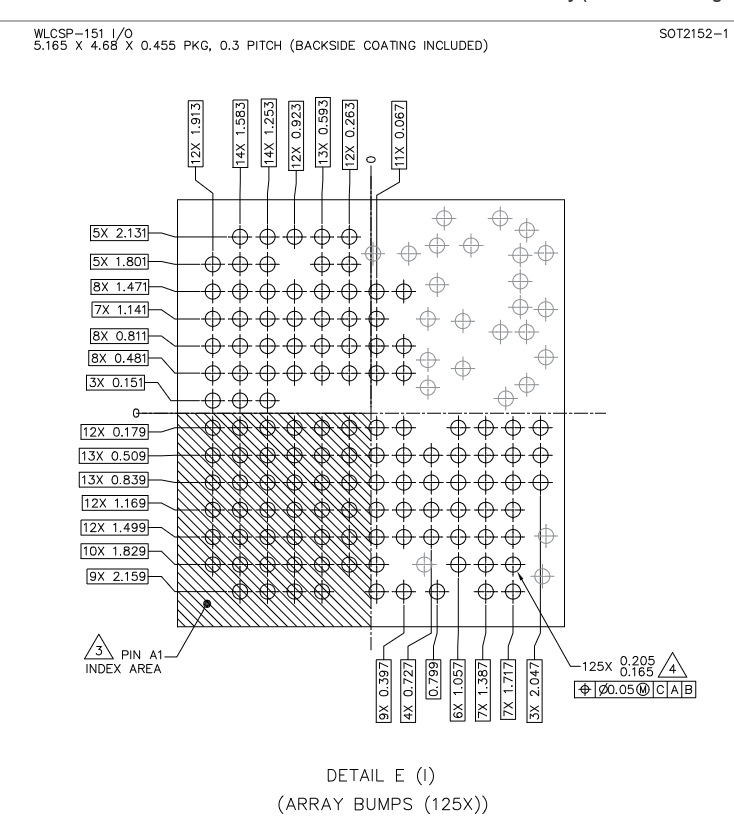
if I read this correctly nxp uses 50µm⌀ openings on their 300µm ICs (edited)
1:58 a.m.
seems really small
Avatar
Assuming (afaik reasonable to do given the pricing fits what I recall as typical for these low end processes) the 2000$/wafer for buying extra undieced wafer(s) is around the marginal per-wafer cost, that'd be a reference price level to compare the plating to, if it's done wafer-at-once in a way that doesn't break the ability to wire-bond dies that expect to get wire-bonded.
2:00 a.m.
(one of the enig siblings is suited to wire bonding on top of the solderable plating; ofc it can't make a thick bump but doing it wafer-at-once means that one doesn't need to hold onto hundreds of tiny dies during the plating process steps)
Avatar
Then you're back to the factory issue
Avatar
Avatar
Jorropo
if I read this correctly nxp uses 50µm⌀ openings on their 300µm ICs (edited)
that's a typical redistribution layer look
Avatar
Do you want to try that ?
Avatar
Avatar
Jorropo
Then you're back to the factory issue
you are a factory
2:01 a.m.
I appreciate the compliment
2:01 a.m.
hum
2:01 a.m.
I'll accept it in the pick and place departement
2:01 a.m.
the enig process is still in developpement kek
2:01 a.m.
to say the least
Avatar
(like, 2000$ isn't insane amounts of value to risk by messing up the plasting process and failing QA, at least after having dialed in the process)
Avatar
I'm gonna test the process on a single IC
Avatar
yes sure
Avatar
Well here is a gap to processing one IC and a wafer
2:02 a.m.
size gap
2:02 a.m.
MarkdownContext { Depth = 1 }
Avatar
I mean once the testing is over and we'd think about replacing the wafer.space 1.5$/chip COB wire bonding add-on with a flip-chip option.
2:03 a.m.
How many chips on one wafer ?
2:03 a.m.
doing some math
2:04 a.m.
I suspect sputtering would be the cheapest, we need like 20µm resolution lihographic capability this sounds doable with an opensource DMD maskless device
Avatar
full slot is 3.93 × 5.12 mm = 20.12 mm²
2:04 a.m.
(that's full die area, not usable-for-transistors)
2:04 a.m.
full wafer is 200mm
2:04 a.m.
why'd we need litho?
Avatar
unlike enig sputtering coats the passivation layer
Avatar
so don't?
Avatar
so you develop a posiive mask over the opening after sputtering
2:05 a.m.
to remove the excess metal
2:06 a.m.
the standard way to make that positive is with litho
Avatar
or is it not enough to turn the exposed shiny aluminium pads into solderable surfaces and then solder like the LGA it turned into?
Avatar
well that the goal indeed
2:06 a.m.
(I don't understand the question)
Avatar
Avatar
namibj
full wafer is 200mm
d or r ?
Avatar
Avatar
Jorropo
d or r ?
d
👍 1
Avatar
The conclusion from the extract is that both are fine ?
2:10 a.m.
Do you want to skip the balls ?
2:10 a.m.
it looks to me like the process for LGA and BGA is identical up until the balls
Avatar
Avatar
Jorropo
(I don't understand the question)
https://discord.com/channels/1361349522684510449/1361349523724570941/1521779301597450271 you see the shiny squares (iirc about or even exactly 40 um squares) along the edges of the die, extending from the same-width structures that ripple through the stripe-y ring that encloses the inner content's grid?
2:12 a.m.
the yellow on the chip except the edge is the passivation layer ?
2:13 a.m.
wait no I get it, that the square in question
2:14 a.m.
this one also very clearly btw.
Avatar
You are talking about the squares right
2:14 a.m.
not the rectangles between the squares ?
2:16 a.m.
@namibj btw how was dinner ?
Avatar
Avatar
Jorropo
not the rectangles between the squares ?
I'm talking about the silvery vey very mirror shiny squares around the very outside edge of the die (technically there's like about half or third of square size gap to the edge, and there's for these dies from Run1 at least an omnipresent narrow (about iirc 1/5th the width of the squares) shiny ring around the entire die on the outside)
Avatar
Avatar
Jorropo
@namibj btw how was dinner ?
tasty
Avatar
Avatar
namibj
tasty
nice
Avatar
Avatar
Jorropo
the yellow on the chip except the edge is the passivation layer ?
yeah
Avatar
Avatar
namibj
I'm talking about the silvery vey very mirror shiny squares around the very outside edge of the die (technically there's like about half or third of square size gap to the edge, and there's for these dies from Run1 at least an omnipresent narrow (about iirc 1/5th the width of the squares) shiny ring around the entire die on the outside)
ok I see it indeed
2:18 a.m.
TIL you can buy 5µm 50k DPI masks for reasonable amount of money, so the sputtering option looks very interesting I only need cleaning + a single chemical bath
Avatar
the edge is the sealring which for dies marked as "wire bonding" has a mandatory exposed strip of metal, which in thse dies is very very close to the squares, which the wire bonding machine doesn't care about but any simple ACF bonding would very much care about.
Avatar
well I also need to get a vastly outdated stepper
Avatar
Avatar
namibj
the edge is the sealring which for dies marked as "wire bonding" has a mandatory exposed strip of metal, which in thse dies is very very close to the squares, which the wire bonding machine doesn't care about but any simple ACF bonding would very much care about.
hum
Avatar
Avatar
Jorropo
Do you want to skip the balls ?
well, we don't need litho to build up solderable plating on the aluminium base.....
Avatar
with sputter you get a single pad (edited)
2:19 a.m.
IC sized pad
2:20 a.m.
if feaures aren't too big I guess you could align a stencil to block the sputtering beam (edited)
Avatar
@namibj I don't know what is your involvement with the project seems high given NXP seems to get by with 50µm openings for balls on the IC do you know where I could some existing open source design ICs ? (that havn't been wire bonded) (edited)
2:30 a.m.
would be enough to try to replicate NXP's setup
2:30 a.m.
given it already has 40µm squares
2:31 a.m.
(well the surface from 40µm to 50µm is a big jump but worth trying)
Avatar
Dense arrays of 60 microns pitch die, with 30 microns pads and 30 microns spacing, were used.
uhhhhhh https://www.techblick.com/post/fine-pitch-direct-die-attach-without-thermal-compression-sunray-scientific
Andrew Stemmerman & John Yundt SunRay Scientific Inc. Eatontown, NJ USAandrew@sunrayscientific.com johny@sunrayscientific.comSunRay Scientific of Eatontown, NJ, USA has developed a new and innovative approach to electronic component assembly.This article will outline the developments of this technology and show examples of this magnetically alig...
Avatar
Avatar
Jorropo
given it already has 40µm squares
if you can deal with the surrounding edge that's like iirc 7 um or so spaced from the square, you could use "any" of the Run 1 dies; I'm not sure who'd most conveniently be able to send you some, but we can see about that in a few days after the tapeout for Run2 closes.
❤️ 1
Avatar
Avatar
namibj
if you can deal with the surrounding edge that's like iirc 7 um or so spaced from the square, you could use "any" of the Run 1 dies; I'm not sure who'd most conveniently be able to send you some, but we can see about that in a few days after the tapeout for Run2 closes.
what is the edge made off ?
Avatar
Avatar
Jorropo
(well the surface from 40µm to 50µm is a big jump but worth trying)
should only have a notable but brute-force-able yield impact; we don't care if the prototypes have say 1% failure per joint
Avatar
MarkdownContext { Depth = 1 }
Avatar
even for 100 pads that's still over 30% yield
Avatar
Avatar
Jorropo
what is the edge made off ?
the same
Avatar
wrong question mb is it passivated ?
2:42 a.m.
enig will coat all the Al
Avatar
as far as the top layher litho is concerned the edge is just a very narrow pad that encloses the entire circuit on the die
Avatar
Avatar
Jorropo
enig will coat all the Al
I know
2:44 a.m.
mask the line under a microscope with a micro manipulator of sorts, and paint it with passivation or such, is what I'd try with Run1 silicon.
Avatar
Avatar
namibj
as far as the top layher litho is concerned the edge is just a very narrow pad that encloses the entire circuit on the die
My current plan is 0. chemical cleaning 1. sputtering 2. spin coating a mask 3. contact mask negative 4. UV 5. chemical bath (remove unwanted sputtered) 6. party just because that is way less chemical bath compared to enig (edited)
2:45 a.m.
I guess ok for testing at least
2:46 a.m.
sputtering isn't easy tho, relatively speaking
Avatar
I'm vastly underequiped tho
Avatar
Avatar
namibj
sputtering isn't easy tho, relatively speaking
sure but I hate chemistry
2:46 a.m.
hate is a strong word
2:46 a.m.
maybe not hate
Avatar
(not that electroless plating baths are particularly stable)
👍 1
Avatar
terrible
2:46 a.m.
I know
Avatar
I don't think you can get by with a single material layer though, to go from the aluminium to something decent for soldering.
Avatar
Ti → Ni → Au
2:47 a.m.
is the classical afait (edited)
2:47 a.m.
the Au is flashed and gets disolved into the tin
2:47 a.m.
from my understanding
2:49 a.m.
@namibj btw did I do the math right is there ~1561 ICs on a single wafer ?
2:51 a.m.
though some are chopped into two for smaller projects/customers
Avatar
Is wafer.space combining 1k different projects on a single MPW run ?
2:51 a.m.
or is the same customer design repeated many times to reach 1k ICs per customer with less wafers ? (edited)
Avatar
no, there's a reticle that gets filled and the facvtory stamps that across the die
2:53 a.m.
afait that reticle is repeated like 40 times on a single wafer ?
Avatar
afaik Run2 has one more row and one more column of half-sized slots so only 18 full-sized slots on the reticle.
Avatar
(I didn't counted the edges weirdness)
Avatar
Avatar
Jorropo
afait that reticle is repeated like 40 times on a single wafer ?
sounds about right; as you could see at the edge it's not quite fully reticle-strict-oriented.
Avatar
Avatar
Jorropo
afait that reticle is repeated like 40 times on a single wafer ?
that seems correct, that makes 25 wafers per MPW (edited)
Avatar
Avatar
namibj
Click to see original message
I thought they always printed half designs because it improved reliability of complete designs (edited)
2:56 a.m.
Avatar
Avatar
Jorropo
I thought they always printed half designs because it improved reliability of complete designs (edited)
it's not worth the litho at the very very edges because there's too much edge close by anyways so the chips aren't too usable anyways; maybe they expose some filler pattern to help the chemical-mechanical-polishing stay more well behaved though, not sure
Avatar
@namibj after some more searching I don't know how NXP is using 50µm opening or if I'm reading that diagram correctly. For 300µm pitch an octogon between 180µm and 100µm diameter should be workable (edited)
2:58 a.m.
I would use 150µm
Exported 226 message(s)
Timezone: UTC+0