Guild icon
wafer.space Community
ℹ️ - Information / general
Welcome to wafer.space - documentation at wafer.space github - buy at buy.wafer.space - archives at discord.wafer.space
Between 2026-06-30 11:59 p.m. and 2026-08-01 12:00 a.m.

Avatar
Avatar
tnt
Need a moderator .. @Leo Moser (mole99) / @Tim 'mithro' Ansell / @Andrew Wingate ?
Tim 'mithro' Ansell 2026-07-01 3:14 a.m.
Was that spam or something else?
👍 2
Avatar
It was spam
7:27 a.m.
❤️ 2
😍 2
Chips4Makers aka Staf Verhaegen started a thread. 2026-07-01 8:10 a.m.
Avatar
quick sanity check before I submit - Should I set the ID to something that's unlikely to clash?
10:15 a.m.
or is that set wafer.space side when the precheck is run?
Avatar
Leo Moser (mole99) 2026-07-01 10:24 a.m.
The precheck does not check it against the other IDs, but the platform should prevent you from choosing an existing ID. The precheck will update the ID macros in your design with your chosen ID.
Avatar
ah, cool.
11:27 a.m.
thank you
👌 1
Avatar
always_ff_rohan 2026-07-01 11:59 a.m.
@Tim 'mithro' Ansell When is the next shuttle run scheduled?
Avatar
I suspect a few weeks after this run has been delivered so people can examine a design and submit an updated version
2:21 p.m.
so about 2 weeks after Early Q4 2026 Bare dies and packaged parts shipped to customers
Avatar
Well at some point runs should be overlapping.
Avatar
Okay, the color NTSC signal generator is coming along really well. It looks like I will be able to generate all the colors, just really badly.
7:14 p.m.
If this works, it’ll make for an interesting single-IO video output option
7:15 p.m.
I’m also going to attempt PAL again, but expect that one to catastrophically break again
7:15 p.m.
I’m not good at making demos, so I’ll continue to just display test patterns
7:15 p.m.
Avatar
Avatar
Tholin
I’m not good at making demos, so I’ll continue to just display test patterns
just adapt one of the demo's that looks good and has a friendly license to your modulator's digital interface?
Avatar
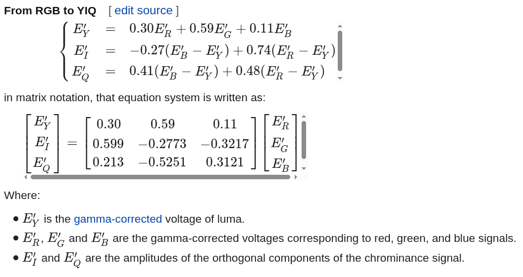
Not really a thing since a RGB to YIQ converter would be too many gates, I think
Avatar
just check it runs at less or equal resolution vs. your modulator's needs, and black box it as necessary
Avatar
Avatar
Tholin
Not really a thing since a RGB to YIQ converter would be too many gates, I think
ehhhh
9:24 p.m.
Avatar
Oops, took me until now to get a repo going https://github.com/AvalonSemiconductors/ws-submission-2026
Multi-project die. Contribute to AvalonSemiconductors/ws-submission-2026 development by creating an account on GitHub.
11:56 p.m.
The functional components are actually done, leaving me with a comfortable two weeks to get the art ready. There is a block of free space on the die reserved for it.
Avatar
@Tim 'mithro' Ansell This is the project I wish to use to officially test my SCL, as well as my multi-project setup using my SCL. I’m also using the level-shifting IO pads, but for having a 5V IO voltage and 3.3V core voltage, which should be interesting. Also has layouts generated by my custom flow tool, analog layouts meant for 3.3V operation and, of course, a bunch of CPUs. Hoping to get a lot of mileage out of this one when it comes to testing things.
💜 2
Avatar
Avatar
carlfk
Click to see attachment 🖼️
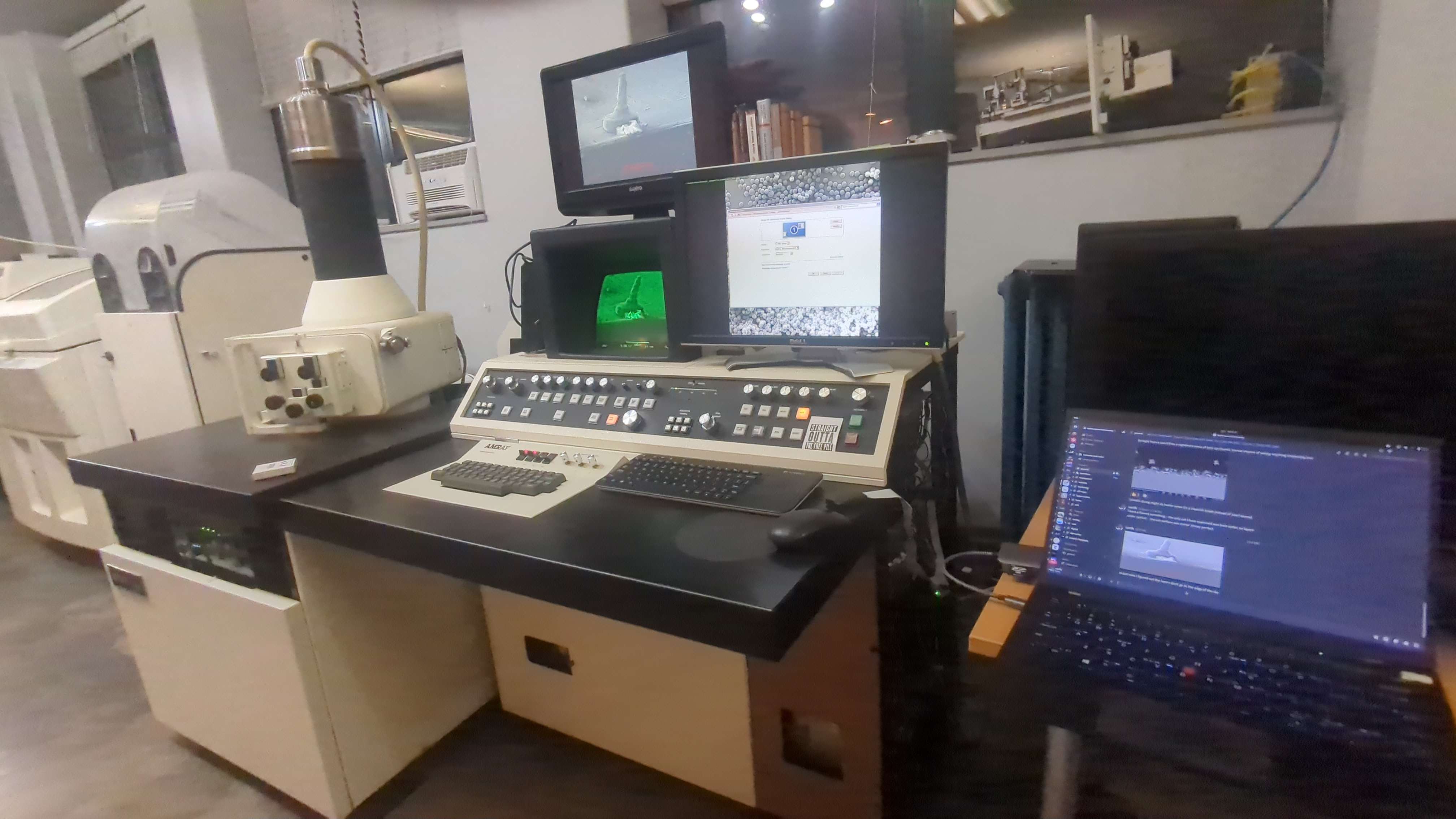
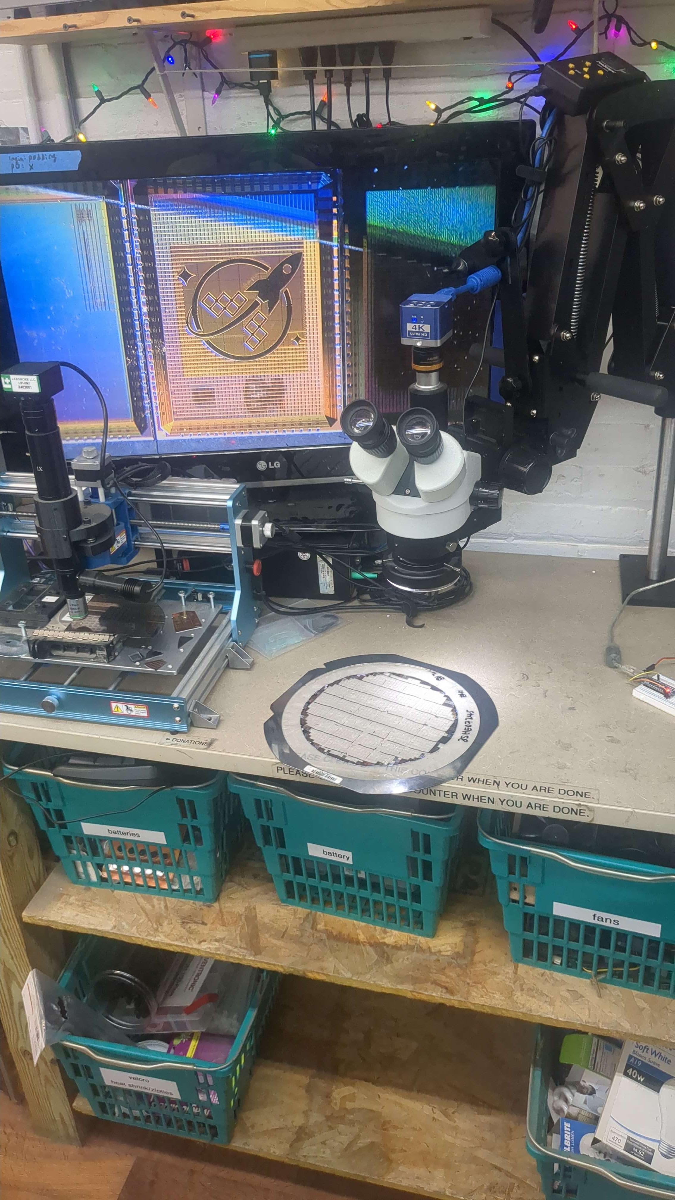
Nice setup
Avatar
I fixed the antenna violations so.... I’m actually done way ahead of deadline for once. This is highly unusual!
💯 2
3:39 p.m.
I’m just waiting for the art now
3:39 p.m.
I guess I’ll just sit here and wait for two weeks, then go get waffles?
Avatar
Leo Moser (mole99) 2026-07-02 4:02 p.m.
In case you're bored, a mux4 would be a great addition to your SCL 😉
Avatar
Avatar
Tholin
I’m not good at making demos, so I’ll continue to just display test patterns
is that in a repo? Ste ps1 guy loves color bars, loves analog and vga. might want to see what you are doing.
7:36 p.m.
oh look, a repo appeared!
Avatar
Avatar
Leo Moser (mole99)
In case you're bored, a mux4 would be a great addition to your SCL 😉
We will see. I am burnt out right now.
Avatar
Avatar
Tholin
I guess I’ll just sit here and wait for two weeks, then go get waffles?
In your position I'd think scripting together a flow of minting a lot of .nodeset's to cover all multistable/regenerative-feedback node voltages,
  • through probably the LVS tooling
  • and some minor singled-out-cell pseudo-DC-op-point sims where you'd start the transient with the regular DC op point initialization as always, then throw whatever waveforms against the inputs that are needed to bring the internal state into the target state, then just stop imposing a maximum step size and let the time integrator run for like an entire simulated minute or so, to then harvest the final state's node voltages from it (for the correct PVT corner! If it's too different one would risk the nonlinear solver potentially skipping across the forbidden band and deciding the flip-flop is actually better off in the opposite state; I do think in principle this could be solved by using the advanced continuation functionality:
the attached user guide's "Figure 8-3" "manual replication of MOSFET contonuation", amended with a 3rd conparam entry that happens after the mosfet:gainscale and mosfet:nltermscale entries, which will be essentially the output conductance of the current-type B-source which hard-forces the stateful digital logic cell's internal node voltage to the reference DC static voltage of the desired internal state of that particular cell, and is ramped from a very high conductance (strong but still sufficciently numerically behaved especially when it comes to transitioning out of the forced state; I'd probably just start with 1 siemens for any vaguely normal CMOS SCL internal nodes) down to literally 0 (which will have it be open-circuit at transient sim runtime). The parameter names legal to put into conparam are the same ones that are also legal to .STEP (the docs for how to casually do .STEP are far far easier to approach/read/understand than the fancy continuation stuffs). .options loca stepper=1 predictor=1 stepcontrol=1 could be semi-necessary to (properly/reliably) handle the effects of combinatorial loops through the (non-transparent at the time of the continuation solving!) flip-flops; if the continuation DC OP point solve ahead of the transient sim itself takes too long it'd be worth testing whether it's sufficciently robust with the tangent predictor 0 and thus the downgrade from the arc-length continuation stepper=1 to stepper=0. Though I guess maybe it has to do continuation over the output resistance and push that out to near-infinity in the continuation solve process (default is like 100 exa); the specified parameter constant value applicable outside of the special circumstances in which the LOCA does continuation on it, will need to be a sentinel (I'd suggest exact 0 or "anything negative"), as it shall be as non-interacting and as sparsified-away by the linear solver and all as possible (it's not a problem because the discintinuity doesn't happen while a non-linear solver tries to solve the system of equations and could have called the behavioral function with node voltages/branch currents far from anythign physical, because that's just discintinuos in a parameter, and that parameter doesn't change during any transient time integration...). Overall the idea I'm proposing is to use gate-level digital sim (post-techmapping (and any retiming and other such intrusive changes to the logic) verilog-sim basically 😄 ) to fast-forward to an interesting moment, snapshot all stateful state, map that against pre-computed DC op points of the cell library, use the LVS matching provisions to match that state to post-PEX SPICE node identifiers, emit a spice file to-be-.include'd full of those continuation-capable cell's-internal-node-forcing B-sources (test if things are faster when forcing combinatorial nets as well, or if the additional effort expended negates the faster convergence; .nodeset is likely cheaper for those though it's just not reliable), and start the .tran sim.

8:16 p.m.
(I can help later next week on the matter if you want; I'm just not at all deep enough int the digital simulation and LVS tooling side to handle that side of this simulation-type-marriage.)
Avatar
Goal IMO would be to (1) test some particularly questionable timing paths that came up in static timing analysis, (2) check if interaction between digital and analog aspects behaves sufficiently well/nicely to not be concerned about mixed-signal features being DOA due to oversights in the analog/digital interface specs, and (3) sanity check that at least normal interaction with any of the non-SCL parts of the chip (any of those) shows no signs of anythign shorting out or being close enough to shorting out to be nearly-equivalent. (I'm still mildy traumatized by how you (not-)handled the excessive current draw/heating of the Run1 die's DAC's buffers.) (The glitching of the video signal you've blamed on the lack of latching of the digital feed to the DACs is actually something I'd file under the above mentioned reason number 2, as it's one thing to accept the glitching if one is aware of it, but a whole nother thing to not have expected it/thought about it being possibly an issue.) (I'm not sure but depending on what you spit out of the NTSC modulator, like in theory there is place for the audio carrier, parts of the functionality are contingent on non-terrible artifacts/interference behavior, as e.g. audio will eventually hurt or at least give headaches if it's bad enough with some artifacts at least.)
Avatar
Avatar
namibj
In your position I'd think scripting together a flow of minting a lot of .nodeset's to cover all multistable/regenerative-feedback node voltages,
  • through probably the LVS tooling
  • and some minor singled-out-cell pseudo-DC-op-point sims where you'd start the transient with the regular DC op point initialization as always, then throw whatever waveforms against the inputs that are needed to bring the internal state into the target state, then just stop imposing a maximum step size and let the time integrator run for like an entire simulated minute or so, to then harvest the final state's node voltages from it (for the correct PVT corner! If it's too different one would risk the nonlinear solver potentially skipping across the forbidden band and deciding the flip-flop is actually better off in the opposite state; I do think in principle this could be solved by using the advanced continuation functionality:
the attached user guide's "Figure 8-3" "manual replication of MOSFET contonuation", amended with a 3rd conparam entry that happens after the mosfet:gainscale and mosfet:nltermscale entries, which will be essentially the output conductance of the current-type B-source which hard-forces the stateful digital logic cell's internal node voltage to the reference DC static voltage of the desired internal state of that particular cell, and is ramped from a very high conductance (strong but still sufficciently numerically behaved especially when it comes to transitioning out of the forced state; I'd probably just start with 1 siemens for any vaguely normal CMOS SCL internal nodes) down to literally 0 (which will have it be open-circuit at transient sim runtime). The parameter names legal to put into conparam are the same ones that are also legal to .STEP (the docs for how to casually do .STEP are far far easier to approach/read/understand than the fancy continuation stuffs). .options loca stepper=1 predictor=1 stepcontrol=1 could be semi-necessary to (properly/reliably) handle the effects of combinatorial loops through the (non-transparent at the time of the continuation solving!) flip-flops; if the continuation DC OP point solve ahead of the transient sim itself takes too long it'd be worth testing whether it's sufficciently robust with the tangent predictor 0 and thus the downgrade from the arc-length continuation stepper=1 to stepper=0. Though I guess maybe it has to do continuation over the output resistance and push that out to near-infinity in the continuation solve process (default is like 100 exa); the specified parameter constant value applicable outside of the special circumstances in which the LOCA does continuation on it, will need to be a sentinel (I'd suggest exact 0 or "anything negative"), as it shall be as non-interacting and as sparsified-away by the linear solver and all as possible (it's not a problem because the discintinuity doesn't happen while a non-linear solver tries to solve the system of equations and could have called the behavioral function with node voltages/branch currents far from anythign physical, because that's just discintinuos in a parameter, and that parameter doesn't change during any transient time integration...). Overall the idea I'm proposing is to use gate-level digital sim (post-techmapping (and any retiming and other such intrusive changes to the logic) verilog-sim basically 😄 ) to fast-forward to an interesting moment, snapshot all stateful state, map that against pre-computed DC op points of the cell library, use the LVS matching provisions to match that state to post-PEX SPICE node identifiers, emit a spice file to-be-.include'd full of those continuation-capable cell's-internal-node-forcing B-sources (test if things are faster when forcing combinatorial nets as well, or if the additional effort expended negates the faster convergence; .nodeset is likely cheaper for those though it's just not reliable), and start the .tran sim.
forgot to attach the file
7:56 p.m.
7:56 p.m.
7:57 p.m.
I apologize for being this late to realize
7:58 p.m.
(that the state of the tooling outside magic is beyond questionable, as it's arguably unacceptable.... it's HORRIBLE do target with klayout unles sone sticks to digital SCL only, and even there tholin knows all too well how not-tuned the tooling is to deal with this process..... antenna violations!)
Avatar
....I guess the teapeout deadline there has now since really taken hold/cemented itself as final
Avatar
I actually have a single unused pad on my die. How unusual.
Avatar
Avatar
namibj
@Thomas Pluck 2.1 do you guys have a functioning nix shell flake with a KLayout where your nice PCells work ?
Thomas Pluck 2.1 2026-07-04 12:57 p.m.
Probably needs to a PR to nix-eda, we don't support this.
Avatar
Thomas Pluck 2.1 2026-07-04 1:24 p.m.
Taking a closer look, you only seem to 3 major semver versions behind - so that might be a start
1:49 p.m.
Not gonna do too many runs. I have to do manual edits to the GDSII file each time.
7:26 p.m.
it can be near the edge - short and only sacrifices a few working die
7:30 p.m.
for imaging attempts.
7:31 p.m.
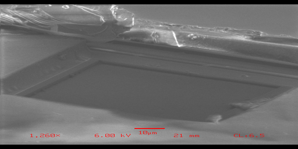
also: if someone can use some of their unused area for some large blobs so that we have an easy target to slice into
7:32 p.m.
regardless of how we cut the die
Avatar
Avatar
carlfk
also: if someone can use some of their unused area for some large blobs so that we have an easy target to slice into
Andrew Wingate 2026-07-04 7:35 p.m.
There are plenty of unusable die near the edges. still whole size, but creep into the exclusion zone
Avatar
Avatar
Andrew Wingate
There are plenty of unusable die near the edges. still whole size, but creep into the exclusion zone
do you have a image of the cut pattern?
7:38 p.m.
I've seen it. can't find it.
7:39 p.m.
either run - or even a fictional run
Avatar
Andrew Wingate 2026-07-04 7:40 p.m.
next run
7:41 p.m.
...maybe
Avatar
fine for me to scribble conctpt art :p
8:25 p.m.
assuming we can get one bonus cut on only one wafer, then one or more of those can add some ... shapes? that the cut will slice
8:28 p.m.
given the timeline, don't need to wait for cut confirmation - just shove the shapes into existing design and maybe something will happen
Avatar
Avatar
carlfk
Click to see attachment 🖼️
Andrew Wingate 2026-07-04 8:31 p.m.
what are you hoping to get from this? you just would get a bunch more half height dies?
Avatar
image it in Peter's SEM (edited)
8:32 p.m.
er.
Avatar
Andrew Wingate 2026-07-04 8:33 p.m.
why not just let me give you some of the scrap ones?
Avatar
this cut will destroy whatever. but I'm assming it will be a nice clean cut. not sure how else to get an edge view
8:33 p.m.
how do we cut?
Avatar
Andrew Wingate 2026-07-04 8:34 p.m.
Ah, I see. you're looking for a cross section of active silicon, not just in the kerf
Avatar
Andrew Wingate 2026-07-04 8:35 p.m.
there are a number of test features that GF puts in the middle of the reticles (the blank spaces) I can just give you that. That's also active
8:35 p.m.
and those are arbitrarily cut as they don't follow our patterns
Avatar
but we don't know what should be there, so we can't verify design vs reality right?
8:37 p.m.
Peter is skeptical we can measure - gonna go play today and see what happens
💜 1
💯 1
Avatar
Andrew Wingate 2026-07-04 8:38 p.m.
I doubt even the edge from a cut that you are suggesting is clean enough to do what you hope it will. At that scale it probably looks like garbage.
Avatar
Avatar
carlfk
Peter is skeptical we can measure - gonna go play today and see what happens
Andrew Wingate 2026-07-04 8:38 p.m.
Looking forward to the results. Make sure Peter puts them somewhere on the internet so people can see them.
Avatar
thats not a thing Peter does :p
😩 1
8:39 p.m.
Ill take a picture of the sceeen with my phone
🤦 1
Avatar
Avatar
Andrew Wingate
I doubt even the edge from a cut that you are suggesting is clean enough to do what you hope it will. At that scale it probably looks like garbage.
yeah there's no way it'll be clean enough for imaging, will definitely need more grinding/lapping to get past the damaged kerf zone. So you'd still need to do some detective work to figure out what part of the circuit you're looking at
💜 1
Avatar
I should probably stop trying to solve a problem I don't have yet
Avatar
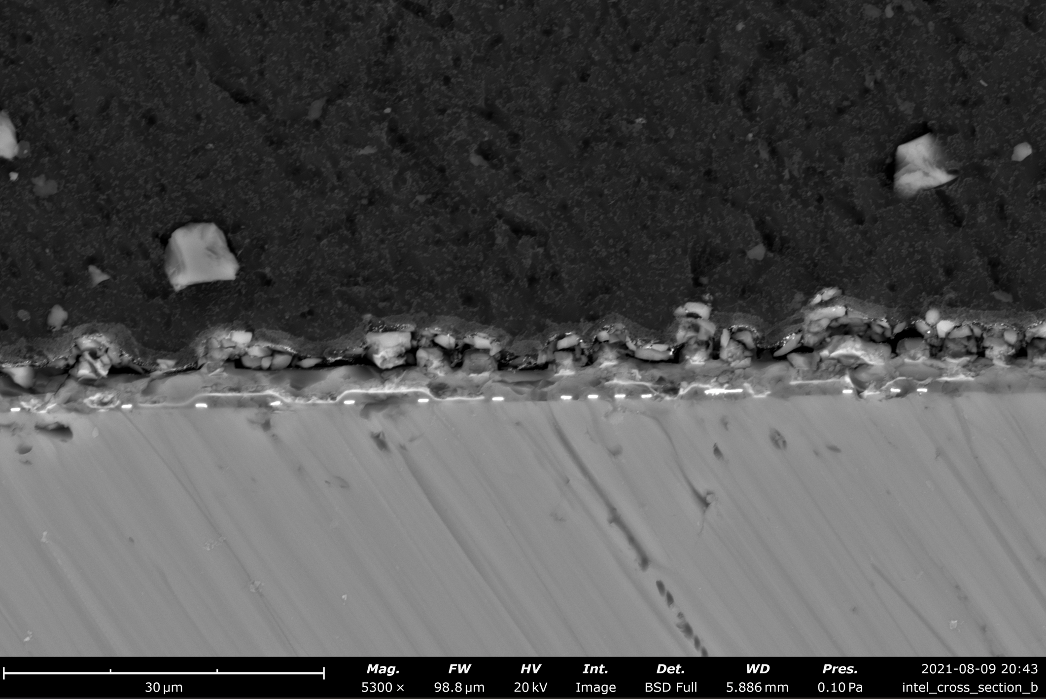
here's a die I cross-sectioned and lapped up to like 2000 grit iirc (something around there). Not particularly careful or good lapping, and the results are notably rough because of it. Silicon bottom, embedding epoxy top. You can see where the silicon tore out and fractured, big furrows from improper lapping through the stages, etc. Straight from a saw it'll be a nightmare mess of torn up chunks, no real chance of seeing anything interesting imo
👍 1
9:13 p.m.
(stealth dicing might do better since it's a clean'ish break instead of saw? dunno)
Avatar
I have a flawed something - the only cut I have examined was bare wafer, no layers
11:18 p.m.
under optical - the cut serface was mirror shiney perfect
5:29 a.m.
so just now I figured out the layers don't go to the edge of the die
5:31 a.m.
Avatar
ima break a w.s die into pieces. any suggestions on how?
Avatar
pinch with channel lock until it breaks into 5+ pieces.
6:30 a.m.
6:30 a.m.
that's a w.s die.
6:34 a.m.
Avatar
@Andrew Wingate is the purchase slots still available to submit clean GDS for 14 July 2026? (edited)
Avatar
Welp, lvs hard, lvs very not optional though 🙁
Avatar
Avatar
Ravi Nataraju
@Andrew Wingate is the purchase slots still available to submit clean GDS for 14 July 2026? (edited)
Tim 'mithro' Ansell 2026-07-05 1:20 p.m.
No, the purchase deadline was 30 June 2026 @ 11:59 PM AoE
👍 1
Avatar
Avatar
carlfk
I have a flawed something - the only cut I have examined was bare wafer, no layers
Tim 'mithro' Ansell 2026-07-05 1:22 p.m.
Package molding Generally epoxy / silica Paddle / Lead Frame Generally copper Silicon die Region with transistors and metal layers Silver conductive epoxy 5x objective ~4 images 10x objective ~8 images
Avatar
Tim 'mithro' Ansell 2026-07-05 1:25 p.m.
Basically, the "structures" are in the very top part of the silicon - like maybe the top <5% or something.
Avatar
Avatar
Tim 'mithro' Ansell
Basically, the "structures" are in the very top part of the silicon - like maybe the top <5% or something.
Tim 'mithro' Ansell 2026-07-05 1:26 p.m.
1:29 p.m.
@carlfk - The Silicon Prawn Discord is probably a good source of advice / hints / etc
Avatar
Avatar
tnt
Click to see attachment 🖼️
If I can help somehow to enable functional extraction for bent-poly-on-comp, including preparing test structures necessary to verify and adjust calibration coefficients from e-test efforts, I'd like to try getting at least something functional into Run2. @Tim Edwards I'd assume the current extraction routines don't put any notable care into dealing with bent-poly-on-comp if they even support that without errors at all?
Avatar
@namibj : Extraction of bent poly might differ slightly from the modeled dimensions, but I put "reasonable" methods into magic for dealing with bends in gates because I have several friends/colleagues who do space-qualified chips and need that extraction for annular FETs. It will calculated the centerline through bends, ignore connecting tabs out to the edge, and if necessary, match differing lengths of segments to obtain a correct effective width.
Avatar
Avatar
Tim Edwards
@namibj : Extraction of bent poly might differ slightly from the modeled dimensions, but I put "reasonable" methods into magic for dealing with bends in gates because I have several friends/colleagues who do space-qualified chips and need that extraction for annular FETs. It will calculated the centerline through bends, ignore connecting tabs out to the edge, and if necessary, match differing lengths of segments to obtain a correct effective width.
Great; if there's anything in particular I could do so we may calibrate that extraction ahead of Run3, that'd be awesome. IIUC, annular fets could maximize the gm/Cd at least at small enough diameters, compared to the classic multi-finger structures (almost) all the open PDK PCells produce for the generic CMOS transistors?
5:24 p.m.
But even then, the image I replied to should already beat the classic finger structure in drain/source junction capacitance, I'd think.
Avatar
@namibj : I am starting a project to make a radiation-tolerant standard cell library using annular FETs for space applications, hoping that (per recent comments on the spASICs page) there will be another opportunity to launch a properly radiation-tolerant microprocessor into space. For now, I am targeting GF180MCU because it's the cheapest option, but I am not going to be ready to have anything on Run 2. I expect to have something ready by Run 3.
💯 1
💜 1
5:29 p.m.
(I am also working on automating insertion of triple-voting registers into LibreLane, and if time permits, I will work on ECC for the SRAM.)
Avatar
Avatar
Tim Edwards
@namibj : I am starting a project to make a radiation-tolerant standard cell library using annular FETs for space applications, hoping that (per recent comments on the spASICs page) there will be another opportunity to launch a properly radiation-tolerant microprocessor into space. For now, I am targeting GF180MCU because it's the cheapest option, but I am not going to be ready to have anything on Run 2. I expect to have something ready by Run 3.
Yeah I wasn't expecting something that big, just some smaller structures that could be used with a combination of extractor and model-parameter tuning, think MOSBIUS-like stuff that could be configured in different ways to exercise the transistors in many ways to gather much more broad calibration data.
Avatar
If you put down some test devices on Run 2 it would be very helpful.
Avatar
Avatar
Tim Edwards
If you put down some test devices on Run 2 it would be very helpful.
Yeah that's kind of my plan I just don't know particularly how they should look, nor what @Tim 'mithro' Ansell has in mind for how they'd need to be interfaced to get e-tested. I'll be busy catching back up with life for the next 2~4 days though, so feel free to think a bit more slowly about what'd seem like a decent idea there. (I'd also love to get shorter-channel native nmos covered if practical, as per previous discussion there are no SPICE models for the 3v3 oxide ones, and the ones for 6v0 oxide stop at fairly long channels under arguments of "but they'd be leaky when off", which to my understanding should be more a question of how far the gate is pulled below threshold than whether their channel dares to go below 1.8μm length.)
Avatar
(I do still wish to understand why the high sheet poly reistors would reasonably need a minimum 1um width; given that they are solely defined by Poly2 drawing in a Resistor zone for width and the spacing of Pplus zones for the contacts at the ends for length; also salicide block needs to overlap the length and current density is limited, but those basically all apply on sky130 as well other than that the minimum width is about half on that.)
Avatar
Could be entirely because the modelling below 1um width is not precise enough.
Avatar
Avatar
tnt
Could be entirely because the modelling below 1um width is not precise enough.
You mean they would "need" their spice models to have an extra bin or two for narrower resistors?
Avatar
I didn't check the spice models at all to see how they are made. But the DRC rules from the gf180 are definitely not all "MR" as-in they are not all hard limits of what they can make. But with wafer.space it makes no difference, they must all be obeyed.
Avatar
Yeah, tbf the only real issues I have there are indeed the hard limit on min width of high sheet poly resistors HRES.2 = 1um and min channel length of native nmos NAT.4 = 1.8um especially (that's for thin oxide) but somewhat also NAT.5 = 1.8 um (for thick oxide), as they just state "(For smaller L Ioff will be higher than Spec)". Besides of course the implied impossibility of a die being designed to support both flip-chip and wire-bond packaging.
Avatar
Avatar
Tim 'mithro' Ansell
@carlfk - The Silicon Prawn Discord is probably a good source of advice / hints / etc
putting chip chips in the sem and looking at them is fairly easy and fun....
7:17 p.m.
but if there is a goal, like measure pad thickness, I need to know what it is
7:18 p.m.
another thing I leaned: it looks like all of the layers stop before the edge. (makes sense)
7:19 p.m.
what would happen if one die had one edge of layers that would get cut into so I have a well defined thing to look at?
Avatar
Avatar
carlfk
what would happen if one die had one edge of layers that would get cut into so I have a well defined thing to look at?
there's a risk for cracks to propagate with that; the bigger problem is likely to argue why that should pass DRC.
Avatar
Avatar
namibj
there's a risk for cracks to propagate with that; the bigger problem is likely to argue why that should pass DRC.
ok, sounds reason enough. im curious: cracks in what? the layers I am guessing?
Avatar
cracks from the snapping-apart-the-silicon-wafer-along-mostly-the-dicing-cut-guiding-of-crack-propagation propagating inwards to the guard ring.
Avatar
I don't understand
Avatar
vertical cracks (the crack's plane's normal being aligned with the dicing line) propagating inwards guided by the layer interface caused by the structures you want existing.
7:40 p.m.
(I don't think that risk is big; but the DRCs we're subjected to are really strict.)
Avatar
the cutting edge "grabbing" the "soft" layers and putting unexpected force where it shouldn't be?
Avatar
more like, the crack in the silicon catching on it and spreading sideways along the structures.
7:46 p.m.
the silicon isn't sawed through; it's scratched and then snapped
Avatar
ah. that. thanks.
7:48 p.m.
@Andrew Wingate I wonder how our samples from Seyrecurse? were diced
Avatar
Avatar
namibj
the silicon isn't sawed through; it's scratched and then snapped
this means my idea of an extra cut though some dies isn't going to help me get a clean edge to image?
Avatar
Andrew Wingate 2026-07-05 7:49 p.m.
same way. I think you may just be thinking that because it looks shiny, it's flat. To a certain extent it is, but under electron microscope it's like the Himalayas
this 1
Avatar
the edge of the silicon looked flat. the layers were a mess, like cement and rebar in a demolished building
Avatar
that said, it shouldn't be too hard to grind/lap down from starting with sufficcient margin, and using suitable shapes visible from top for alignment.
Avatar
it looks like more effort than I want to put into it just for the fun of it - this is why I want a well defined goal with some value
Avatar
(not easy, but getting down to like 50nm roughness isn't that unusual for mildly fancy optical lapping)
Avatar
if you want to send samples, I'm happy to image them.
7:54 p.m.
we should have an #image channel here that I can just dump the "this looke neet" and "here is 5 shots of the same thing"
Avatar
IMO what might be more interesting is looking at some finer cornering/zig-zag/patterned structures on the lower layers (m1/m2 but especially also poly2 and the STI edges at comp) by lapping the BEOL gradually down
Avatar
I live stream of the monitor isn't out of the question. it has even been floated to let people remotely be on speaker phone directing the SEM operator (me)
💜 1
💯 1
Avatar
Avatar
Tim Edwards
@namibj : I am starting a project to make a radiation-tolerant standard cell library using annular FETs for space applications, hoping that (per recent comments on the spASICs page) there will be another opportunity to launch a properly radiation-tolerant microprocessor into space. For now, I am targeting GF180MCU because it's the cheapest option, but I am not going to be ready to have anything on Run 2. I expect to have something ready by Run 3.
this is a very cool project! Excited to see/read more when you get into it
Avatar
Avatar
Ravi Nataraju
@Andrew Wingate is the purchase slots still available to submit clean GDS for 14 July 2026? (edited)
Looks like @Tim 'mithro' Ansell already gave you an answer. Fear not! We're hoping to accelerate our cadence and hope to have Run #3 with a GDS in date sometime in Dec 2026 So you can plan for that in the very near future!
👍 2
🎉 1
Avatar
Avatar
Nino_Y
Hi everyone, has anyone ever used cadence's tool instead of librelane flow?
Tim 'mithro' Ansell 2026-07-06 1:11 a.m.
I believe @peterkinget's team might have tried it. However, wafer.space provides no type of support for this and your design must be clean by the wafer.space platform check, not whatever cadence claims.
Avatar
Avatar
carlfk
Click to see attachment 🖼️
Tim 'mithro' Ansell 2026-07-06 1:16 a.m.
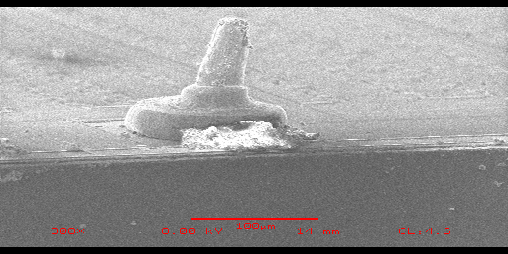
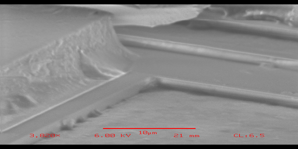
@Andrew Wingate / @Lauri - I wonder if @carlfk could take some images of bad bonds to give us more information about what is going on when they fail?
Avatar
Avatar
namibj
Yeah that's kind of my plan I just don't know particularly how they should look, nor what @Tim 'mithro' Ansell has in mind for how they'd need to be interfaced to get e-tested. I'll be busy catching back up with life for the next 2~4 days though, so feel free to think a bit more slowly about what'd seem like a decent idea there. (I'd also love to get shorter-channel native nmos covered if practical, as per previous discussion there are no SPICE models for the 3v3 oxide ones, and the ones for 6v0 oxide stop at fairly long channels under arguments of "but they'd be leaky when off", which to my understanding should be more a question of how far the gate is pulled below threshold than whether their channel dares to go below 1.8μm length.)
Tim 'mithro' Ansell 2026-07-06 1:19 a.m.
https://bit.ly/test-open-pdk has the spec for pads which where used on SKY130 by @Mehdi and NIST for the data in https://github.com/google/skywater-pdk-sky130-raw-data and would probably be good to follow.
Test structure generation and measurement For improving open source PDKs bit.ly/test-open-pdk Owner: Tim ‘mithro’ Ansell <me@mith.ro> Contributors: XXX Last Updated: 2023 Q1 Goal The goal of this document is to provide a central point for the (automated) development of test structures and...
Raw data collected about the SKY130 process technology. - google/skywater-pdk-sky130-raw-data
Avatar
Avatar
Tim 'mithro' Ansell
@Andrew Wingate / @Lauri - I wonder if @carlfk could take some images of bad bonds to give us more information about what is going on when they fail?
Andrew Wingate 2026-07-06 1:19 a.m.
I don't think I have any dies that have been tested, but I'd be happy to facilitate.
Avatar
Avatar
carlfk
putting chip chips in the sem and looking at them is fairly easy and fun....
Tim 'mithro' Ansell 2026-07-06 1:20 a.m.
One of the things we wanted to look at/confirm was the top metal thickness -- I believe we are unsure if we ended up with the 11 thousand or 9 thousand angstrom thickness for that layer.
Avatar
Notably I'm thinking of using structures with more than 3 pads (+substrate) involved, or at least more than 1 transistor involved, as AFAIK we do have access to model fitting tools through Sandia's Ron.
Avatar
Avatar
carlfk
it looks like more effort than I want to put into it just for the fun of it - this is why I want a well defined goal with some value
Tim 'mithro' Ansell 2026-07-06 1:23 a.m.
For the cross sections we did of the cypress parts with @digshadow, I think the "lapping" was done by hand with a very fine sandpaper and that turned out pretty great. https://x.com/johndmcmaster/status/1715863105782378529?s=20
Skywater SKY130FD integrated circuit cross section. You can see the layers that make up a chip including the metal wiring and transistors!
😍 1
Avatar
Avatar
Andrew Wingate
I don't think I have any dies that have been tested, but I'd be happy to facilitate.
Tim 'mithro' Ansell 2026-07-06 1:23 a.m.
Maybe coordinate with Lauri? I guess we would need to figure out how to ship the die which have not been expoxied or something?
Avatar
Andrew Wingate 2026-07-06 1:24 a.m.
ooh.. no epoxy? Think that's necessary?
Avatar
It'd be important to know if we could drop to the finer pitch of layers regardless of the secondary implants for some test devices at least; think 0.28 L thick oxide structures and just-sub-1.8L nvt NMOS. And narrower-than-1.0 high sheet poly. I'm well aware none of those currently have SPICE models; but it's infeasible to get those SPICE model bin parameters without rather proprietary information and 3D TCAD, or by doing test structures and running model fitting on those.
1:30 a.m.
If that's something we'd have to prepare and submit with a replacement on hand that didn't exceed the open PDK in any way, that'd of course be fine.
Avatar
The epoxy isn't strictly necessary but you're going to have a much better time with it. I would recommend it if you can
Avatar
Oh I had cursed ideas for octagonal symmetry of a device with one drain, one source, 17 gate contacts (or 25 for symmetry, likely), and arguably 25 distinct channels in the BSIM extraction. A big part of it's usability would be contingent on the fab managing to manufacture "decent" matching across the (rotational) symmetry, which probably starts off mildly restrictive from the 5nm coordinate grid interacting poorly with that pesky sqrt(2) aspect, considering "mere" 300nm channel lengths. Also I'm actually not too sure it's appropriate to run that with the 25th channel doing anything beyond power gating, sadly.
11:17 a.m.
(I'm fairly confident though that structure would result in substantially lower parasitic drain side capacitance and lower excess field poly capacitance of the gate contact pads.)
Avatar
Avatar
Tim 'mithro' Ansell
https://bit.ly/test-open-pdk has the spec for pads which where used on SKY130 by @Mehdi and NIST for the data in https://github.com/google/skywater-pdk-sky130-raw-data and would probably be good to follow.
Ahhh ok I'll go through the links in there later; do you have any guidance on whether to expect getting finer structures (than what are almost certainly electrically motivated DRC clauses) allowed for extending the SPICE models down towards manufacturing minimums; in particular (unless someone tells me the FETs would be useless from short channel effects at that point): 1. thick oxide gates shaped like their thin oxide brethens (I'd assume they'd have substantial DIBL together short-channel-typical reduction in general threshold voltage), 2. native threshold voltage NMOS with lengths between normal threshold voltage minimums (0.28~0.6~0.7) and the current NAT.4/NAT.5 minimum 1.8, 3. Un-salicided poly resistors narrower than the (I can only presume matching/process-control related) existing coded minimum widths: PRES.1 (0.8), LRES.1 (0.8), HRES.2 (1.0), 4. Y.PL.2 mentions 0.13 drawn channel length on thin oxide; I assume the short channel effects (possibly HCI) are generally considered too severe for other usage, but it's vendor lock to Yield Microelectronics Corporation is similarly restrictive to open source EEPROM on gf18mcuD as the proprietary-core-only tiny transistors on sky130 are to dense open source SRAM. Like I wish I understood better what's keeping us from being allowed marking layers to not have to bother their engineers about structures that land between electrically recommended sizing and what the lithography can manufacture without risking damage to equipment or the rest of the wafer. Could it be that some of this is from "Google-sponsored-runs" open PDK philosophy where the DRC co-writer (Google) had incentive to keep designers from submitting chips that don't work?
Avatar
Avatar
carlfk
I live stream of the monitor isn't out of the question. it has even been floated to let people remotely be on speaker phone directing the SEM operator (me)
Could you perhaps help us quantify how "necessary" the full guard ring structure turns out to be? I'd think we'd be able to fit some questionable guard structures along some edge that goes to the overflow zone of the reticle (the reticle seems to not be evenly divided by the slot grid along the AFAIK vertical direction of the slot size), in particular the currently forced exposure of the guard ring top metal which is very close to the wire bond pad ring's exposed top metal and not doing that would seem to allow for some cheap flip-chip options that rely on a reasonable minimum spacing between exposed top metal to not require high-end lithography to contact only one pad each.
Avatar
Avatar
namibj
Could you perhaps help us quantify how "necessary" the full guard ring structure turns out to be? I'd think we'd be able to fit some questionable guard structures along some edge that goes to the overflow zone of the reticle (the reticle seems to not be evenly divided by the slot grid along the AFAIK vertical direction of the slot size), in particular the currently forced exposure of the guard ring top metal which is very close to the wire bond pad ring's exposed top metal and not doing that would seem to allow for some cheap flip-chip options that rely on a reasonable minimum spacing between exposed top metal to not require high-end lithography to contact only one pad each.
help how? I have access to a friend's SEM, don't know much about ic design
Avatar
Avatar
carlfk
help how? I have access to a friend's SEM, don't know much about ic design
By helping us figure out what the structures would need to do/how they could be design-for-testing, so we could get that data on how critical these aspects of the guard ring are to the resulting chip yield, without the immense expense of brute force testing. I can't write much rn though.
Avatar
about all I have to offer: prep is tricky, it would help if the slice was at or near the edge
5:07 p.m.
and now is the time to add some stuff specifically for looking at when it comes back from the fab in 3 months
Avatar
Avatar
carlfk
and now is the time to add some stuff specifically for looking at when it comes back from the fab in 3 months
Yeah, basically it's apparently something about cracks and potential of contaminants diffusing through a gap in a metal layer due to the dielectric filler being more vulnerable there than it would be between the vias?
Avatar
Avatar
carlfk
about all I have to offer: prep is tricky, it would help if the slice was at or near the edge
I'm pretty sure it'd be quite straight forward to get much of that manual stuff automated.
Avatar
one thing about the SEM - it takes a min or two to attach the sample to the stage (special carbon something double sided tape) another min to load the sage into the chamber. 2 min (maybe more) to pull a vacuum. so easy 5 min before anything shows up.
5:28 p.m.
I would be surprised if a sample can be removed and lapped a little more
5:29 p.m.
so any iteration of remove material and looking at the slice to see if it is good isn't going to happen in the SEM
Avatar
Avatar
carlfk
so any iteration of remove material and looking at the slice to see if it is good isn't going to happen in the SEM
Yeah I know.
Avatar
@Mod more spam
👍 1
Avatar
fwiw I added a channel to my discord that auto-bans anyone who posts in it (using a bot). not perfect but it seems to catch a lot of those driveby bot spams
💜 1
Avatar
Avatar
BreakingTaps
fwiw I added a channel to my discord that auto-bans anyone who posts in it (using a bot). not perfect but it seems to catch a lot of those driveby bot spams
Andrew Wingate 2026-07-06 9:50 p.m.
Is it open? Want to share a link?
Avatar
Avatar
Rob Taylor
I'd like to announce the first official release of Jacquard - a GPU accelerated, timing aware and gate-level capable simulator. Apple GPU, NVIDIA and AMD are supported (though AMD less tested due to lack of github runners) It currently has support for gate level simulation of SKY130 and GF180 standard cells, and the upcoming 0.3 will be able to support any cell library. I've been using it for my recent wafer.space designs 😁 Please dig in and report any issues!
Tim 'mithro' Ansell 2026-07-07 1:50 a.m.
There are a few groups from TensTorrent lurking on this Discord, maybe you can convince them to collaborate on something. I know they use ventilator internally on some stuff.
Avatar
(oh man, I was inches from purchasing a tenstorrent card the other day. looks like a really fun architecture to program) (edited)
Avatar
Tim 'mithro' Ansell 2026-07-07 7:15 a.m.
@BreakingTaps / @Rob Taylor - The fix for Google Drive, Dropbox and Fastmail download has been deployed to https://platform.wafer.space now.
Platform for wafer.space low cost silicon manufacturing.
👍 3
7:16 a.m.
The https://platform.wafer.space also now has the ability to select the CoB packaging and the CrowdSupply order number on your project. Will put an announcement in #announcements with some other updates shortly.
Platform for wafer.space low cost silicon manufacturing.
👍 2
Avatar
moderator : Spam ... ( @Tim 'mithro' Ansell @Leo Moser (mole99) )
👍 1
urish started a thread. 2026-07-07 1:11 p.m.
Avatar
Tim 'mithro' Ansell 2026-07-07 2:55 p.m.
🔥 1
Avatar
algofoogle (Anton Maurovic) 2026-07-07 4:24 p.m.
Howdy folks, I did a brief video of a wafer.space Tiny Tapeout chip (experimental "ttgf0p2") that I was lucky enough to participate in, and even luckier to try out. This is just a teaser, and I hope to share more soon: https://www.linkedin.com/posts/anton-maurovic_asic-openasics-activity-7480291900114030592-cFQw?utm_source=share&utm_medium=member_desktop&rcm=ACoAACUSJDsBhWb3XdMIrld_0q8cMtLDXdKRF8s
I've been busy since my last post! A dozen more personal #ASIC projects taped out that I'm keen to share soon, but for now here's a teaser of an experimental Tiny Tapeout chip I received from wafer.space's Tim Ansell and have been playing with. Making #OpenASICs never gets old, but now the silicon is coming back in waves and I've got to test mor...
🎉 2
❤️ 1
4:25 p.m.
Thanks @Tim 'mithro' Ansell for the chip! It's a beauty. And well done to the Tiny Tapeout team, of course.
🫂 1
Avatar
Hi. I’m starting to work with GF PDK and was wondering about the 6V transistors and 10V LDMOS. Are they available in the shuttles?
Avatar
the latter aren't easy to use; the former are just longer channel vversions of the 5V types, with no real further differences besides that increased minimum channel length (and maybe a few other DRC minimums)
Avatar
Avatar
namibj
the latter aren't easy to use; the former are just longer channel vversions of the 5V types, with no real further differences besides that increased minimum channel length (and maybe a few other DRC minimums)
I’ve worked with LDMOS before, that’s why I’m interested in those. How can I enable them in the PDK, especially in KLayout?
Avatar
...yeah, on another matter, as you aren't the only one trying to use them, does anyone have PCells on hand for the gf180mcuD LDMOS (the 10V devices)?
Avatar
Avatar
namibj
...yeah, on another matter, as you aren't the only one trying to use them, does anyone have PCells on hand for the gf180mcuD LDMOS (the 10V devices)?
I see, there are not PCells available yet. That is good information, thanks!😊
Avatar
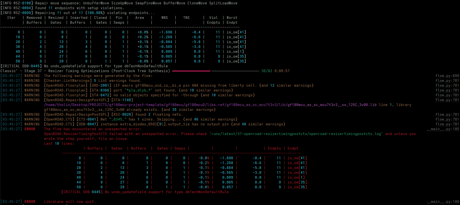
Alright, ya’ll can have some mux4 as a treat!
🎉 3
🥳 1
Avatar
Now the question is how long will that take to filter through to the project template and should I rebuild TinyQV using it? TQVD is squeezed to the limit of what I can fit into it at the moment so it could help a bit.
Avatar
It is taking approximately three eternities to characterize, because its a 6-input function (edited)
7:35 p.m.
(one eternity for each process corner)
😆 2
Avatar
I had to disable mux4_2 from synthesis, because its causing issues in timing repair
😢 1
1:46 a.m.
Avatar
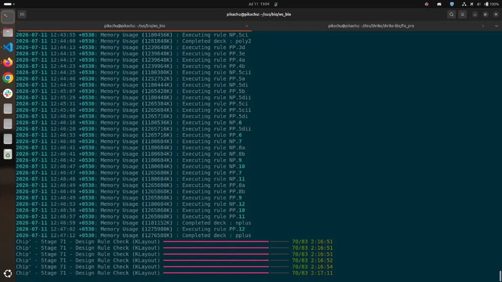
I am facing this issue where the flow just gets stuck here after the klayour-drc after the deck has finished ( the magic one ended without error) does anyone have any ides about this . Its been stuck there for a 1 hour now so that not supposed to happend . also checked on cpu there is no klayout running . I am on latest template . also i want to know is it possible to restart the flow from this point if i kill it or have to run again (edited)
Avatar
DRC can take 3-4 hours depending on machine. If you don't have enough RAM and start swapping that could get longer.
Avatar
Avatar
Tholin
Alright, ya’ll can have some mux4 as a treat!
Question: would use of 45 degree bends of poly2 on comp have helped you on any of the cells so far?
Avatar
I don’t think so
Avatar
I'll see to get the octagonal and the related quadratic structure drawn up now; so that I can do the write-up for them on my travel (to a meetup, in a little bit, basically as soon as I'm done with that).
Avatar
Avatar
tnt
Click to see attachment 🖼️
@Tholin note this tactic does work for gf18mcuD.
Avatar
The main bottleneck is actually how many metal1 traces I can have running in parallel
namibj started a thread. 2026-07-11 5:27 p.m.
Avatar
Does LibreLane throw any kind of error if it detects a VDD/VSS short anywhere?
Avatar
If it detects it ... sure. But by default the LVS is abstract so depending on where the short comes from it could be missed.
Avatar
Avatar
Tholin
Does LibreLane throw any kind of error if it detects a VDD/VSS short anywhere?
Are you worried about a chip being DOA?
10:16 p.m.
I have the FeatherLane generated layouts on there
Avatar
Avatar
Tholin
Click to see attachment 🖼️
After determining that this issue is caused by quirks of this specific design, I’m re-enabling mux4_2 for synthesis
Avatar
Avatar
Tholin
Sortof?
I can see to get extraction running through the recently (weeks) improved magic PEX and get Xyce to solve at least DC op point for it, if you want?
Avatar
(I take a .gds, of which I expect to have to delete all labels but the pad labels myself, followed by fully flattening it. If you have any conventions on pad labeling, I'd prefer those to be applied already and this includes separating the VDD and the VSS pads individually.)
Avatar
Multi-project die. Contribute to AvalonSemiconductors/ws-submission-2026 development by creating an account on GitHub.
10:35 p.m.
There’s two in there. Use the GDSII files. fl_mcpu32 is way smaller, test with that
Avatar
I'm ETA about 40 minutes from my desk.
10:40 p.m.
I hope magic 8.3.674 is pretty recent?
Avatar
Avatar
Tholin
There’s two in there. Use the GDSII files. fl_mcpu32 is way smaller, test with that
How is that to be biased/connected?
10:43 p.m.
Answer only needed if not obvious from looking.
Avatar
You can look at the .v files to see what is an input and an output
10:43 p.m.
If you wanna just do DC, tie all inputs low (edited)
10:44 p.m.
If you want to check if the outputs are outputting, you may do that.
Avatar
Avatar
namibj
(I take a .gds, of which I expect to have to delete all labels but the pad labels myself, followed by fully flattening it. If you have any conventions on pad labeling, I'd prefer those to be applied already and this includes separating the VDD and the VSS pads individually.)
There's a series of commands in magic that will flatten the layout but ignore the text. I don't think you need to prepare a flattened version outside of magic. (edited)
Avatar
Avatar
bailey
There's a series of commands in magic that will flatten the layout but ignore the text. I don't think you need to prepare a flattened version outside of magic. (edited)
Oh, good; I'd need hand-holding magic just confuses me 🙁
10:53 p.m.
(I'll proceed to use the same tactic as last time, provided this is with a padframe.)
Avatar
Avatar
namibj
Oh, good; I'd need hand-holding magic just confuses me 🙁
This magic manual page describes the 2 magic pex extraction flows. Search for PEX http://www.opencircuitdesign.com/magic//howto.html One with just capacitances and one with resistors and capacitances.
Avatar
Ahh I'll just take only the m4 labels
👍 1
Avatar
Avatar
Tholin
There’s two in there. Use the GDSII files. fl_mcpu32 is way smaller, test with that
Avatar
Avatar
bailey
This magic manual page describes the 2 magic pex extraction flows. Search for PEX http://www.opencircuitdesign.com/magic//howto.html One with just capacitances and one with resistors and capacitances.
I got a script around that wrangles it through.
Avatar
Avatar
namibj
Click to see attachment 🖼️
.subckt fl_mcpu32 VSS VDD le clk rst_n rst_override_n din[0] clk_n din[11] din[10] + din[9] din[8] din[7] din[6] din[5] din[4] din[3] din[2] din[1] din[12] din[13] din[15] + din[14] address[0] address[1] address[11] address[7] address[8] address[6] address[4] + address[3] address[13] address[14] address[12] address[9] address[2] address[15] + address[10] address[5] dout[1] dout[2] dout[3] dout[4] dout[5] dout[6] dout[7] dout[15] + dout[14] dout[13] dout[12] dout[11] dout[10] dout[9] dout[8] dout[0] oeb bus_enable + web unused[0] unused[1] unused[2] unused[3] unused[4] unused[5] unused[6]

Avatar
Avatar
namibj
Click to see attachment 🖼️
Avatar
``` Netlist error in file tb_fl_mcpu32.xyce at or near line 15 Model is required for device D0 and no valid model card found. ``` great!
11:59 p.m.
looks like diode models need explicit importing as library....
12:00 a.m.
* Device Count Summary ... C level 1 (Capacitor) 280984 D level 1,2 (Diode) 9694 M level 14 (BSIM4) 44848 R level 1 (Resistor) 267528 V level 1 (Independent Voltage Source) 22 --------------------------------------------- Total Devices 603076 * Setting up matrix structure... * Number of Unknowns = 292543 * Initializing... Analyzed Singleton Problem: --------------------------- Singletons Detected! Num Singletons: 44 --------------------------- ConstructedSingleton Problem: --------------------------- RatioOfDimensions: 0.99985 RatioOfNonzeros: 0.765899 --------------------------- ZOLTAN Load balancing method = 10 (HYPERGRAPH)
12:01 a.m.
(that's the small one; the large one is still extracting)
Avatar
Oh, so that’s what that happens! I usually just remove the diodes from the netlist.
Avatar
Avatar
Tholin
Oh, so that’s what that happens! I usually just remove the diodes from the netlist.
(Yeah it's LLM-prepared; minor manual edits have been done to it; nothing about this testbench seemed too complex to be likely to break and it's hot here... really hot, for 2:30 am.)
12:31 a.m.
mayhaps continuation=2 (natural MOS parameter homotopy) was not the efficcient thing to do, for as it's still stuck on the same screen/output as shown above.)
12:34 a.m.
let's try without continuation and to directly solve for the 3.3V case.
12:38 a.m.
(affording the 2.5 + 1.7 GB of ram usage for the continuation attempt, I've paused that and am trying now without continuation.)
12:40 a.m.
(maybe full-die PEX usage is actually only for cluster usage... hmmmpf)
namibj started a thread. 2026-07-12 12:57 a.m.
Avatar
There is no need to to PEX ...
6:32 a.m.
You can instruct librelane to use GDS for LVS instead of DEF and then the LVS will actually check submodules instead of abstracting then. And you can double check that in the report.
Avatar
Tim 'mithro' Ansell 2026-07-12 11:00 a.m.
Avatar
Avatar
Tim 'mithro' Ansell
Click to see original message
https://discord.com/channels/1361349522684510449/1523053835864637510/1524075766219014326 @RebelMike is the free edge possibly free of top metal, and as such possibly suited for putting flip chip bond pads there?
Avatar
Avatar
namibj
https://discord.com/channels/1361349522684510449/1523053835864637510/1524075766219014326 @RebelMike is the free edge possibly free of top metal, and as such possibly suited for putting flip chip bond pads there?
metal5 is used for power rails, so there's probably not loads of space. But if you want to try and prove some flip chip bonding method maybe it would be better to make a test project where you didn't need most of the pads to work in order to get anything useful out? If Tim thinks that is an interesting project it might get accepted by the sounds of things
Avatar
Yeah so, the thing is, most of the chip would be barren if only housing connectivity (4-wire kelvin measurements) test pads. And in this time I can't get much interesting structure done below, sadly, especially given that I'm not allowed to test vaguely-short channel native nfet's because someone decided years ago what amount of subthreshold leakage would be permissible to design with, and banned all channels narrower than that. Though I guess I should check again if the 0.5um channels would pass DRC.
Avatar
Avatar
RebelMike
metal5 is used for power rails, so there's probably not loads of space. But if you want to try and prove some flip chip bonding method maybe it would be better to make a test project where you didn't need most of the pads to work in order to get anything useful out? If Tim thinks that is an interesting project it might get accepted by the sounds of things
Oh I see now. Would that chip need more than one VDD/VSS pair per SRAM tile? Even if, feeding the m4 straps both at the bottom and the top of each tile (or like, connecting the m4 through and putting a shared m5 connection at the border between SRAM tiles, freeing up m5 over the active memory region), that would give plenty of freedom for some varied pad designs. Also would conveniently test "circuit under [flip-chip] pad".
Avatar
How fast are the available IO pins? The possibility of free silicon is almost irresistable but I think the best path I'd have to doing something relatively cool would be to use my ethernet library. Unfortunately I only have RGMII support, so i'd need 125MHz IO 🤔
Avatar
Avatar
namibj
Oh I see now. Would that chip need more than one VDD/VSS pair per SRAM tile? Even if, feeding the m4 straps both at the bottom and the top of each tile (or like, connecting the m4 through and putting a shared m5 connection at the border between SRAM tiles, freeing up m5 over the active memory region), that would give plenty of freedom for some varied pad designs. Also would conveniently test "circuit under [flip-chip] pad".
Feeding power to those SRAMs is a bit tricky as they ideally need connections around their edges. I'm in the final stages of finishing this design so don't really want to be messing with things, but I'm not paying for it so if Tim/Leo would like to dedicate some area to a flip chip pin test I could potentially just remove some of the SRAMs if you had a macro that would drop in their place. I'm pretty sure the PDN grid will just drop some straps if you block met5, which maybe isn't ideal for power distribution integrity, but probably also not a disaster. And if you had a ready to go macro i would also be easy for someone to drop into a different design.
Avatar
Avatar
RebelMike
Feeding power to those SRAMs is a bit tricky as they ideally need connections around their edges. I'm in the final stages of finishing this design so don't really want to be messing with things, but I'm not paying for it so if Tim/Leo would like to dedicate some area to a flip chip pin test I could potentially just remove some of the SRAMs if you had a macro that would drop in their place. I'm pretty sure the PDN grid will just drop some straps if you block met5, which maybe isn't ideal for power distribution integrity, but probably also not a disaster. And if you had a ready to go macro i would also be easy for someone to drop into a different design.
I mean in principle the edges would be free? The wiring would ideally be escaped somehow to an e.g. ESD diode or something.
Avatar
Avatar
TheZoq2
How fast are the available IO pins? The possibility of free silicon is almost irresistable but I think the best path I'd have to doing something relatively cool would be to use my ethernet library. Unfortunately I only have RGMII support, so i'd need 125MHz IO 🤔
That should work.
1:42 p.m.
Re: ready-to-go macro: basically I'm hoping to test a few mostly pairs of pads of sufficciently varied size and pitch, primarily targeting the "ACF + JLC's special 2L 0.33oz (each) flex" affordable baseline.
Avatar
Avatar
TheZoq2
How fast are the available IO pins? The possibility of free silicon is almost irresistable but I think the best path I'd have to doing something relatively cool would be to use my ethernet library. Unfortunately I only have RGMII support, so i'd need 125MHz IO 🤔
I think the best answer we have is: probably. A 200MHz input clock worked ok. The outputs are strong so likely to work at that speed, but as far as I know I don't think anyone has tried anything non-trivial running at a fast clock in run 1.
Avatar
Yeah not sure how fast the 3v3 library is in practice, but the foundry 5V library even the 9T one is apparently fairly slow.
Avatar
Cool, I might give this project a shot then 🤔
Avatar
Indeed - the challenge will likely be more in driving the logic that fast, not the speed of the IO pads
Avatar
Avatar
TheZoq2
Cool, I might give this project a shot then 🤔
IMO prepare to immediately put a DDR serdes by the IO pads without much routing, drop down to at least 4 if not 8 wide per-IO-lane; then your core should likely have no severe issues synthesizing to timing.
1:51 p.m.
@RebelMike For the record, a major practical use case I'm hoping to prove viable with this is putting more than one flip chip pad on a standard-size TT analog tile, i.e., on that 340x325um area, and in a way that can be extended sideways to cover up to maximum-size analog tile. So we're not talking about large areas here, for the most part at least.
Avatar
I think this is my most scuffed tapeout so far, seeing as I have to make manual edits in KLayout to the top-level GDSII to fix DRC errors.
😬 1
Avatar
I had to do a emergency hotfix in my SCL to un-do an earlier change that introduced a bug that broke synthesis! If anyone is using my SCL and using the latest build from my GitHub, update, and re-run all your flows!
Avatar
Avatar
Tholin
I had to do a emergency hotfix in my SCL to un-do an earlier change that introduced a bug that broke synthesis! If anyone is using my SCL and using the latest build from my GitHub, update, and re-run all your flows!
noob question: what's an SCL ? (edited)
Avatar
standard cell library
👌 1
Avatar
судонет 2026-07-13 8:35 a.m.
yay!!!
8:36 a.m.
my 16-bit risc cpu is manufacturable!!!
👏 5
8:41 a.m.
all in a few days' work, i guess* (edited)
Exported 265 message(s)
Timezone: UTC+0