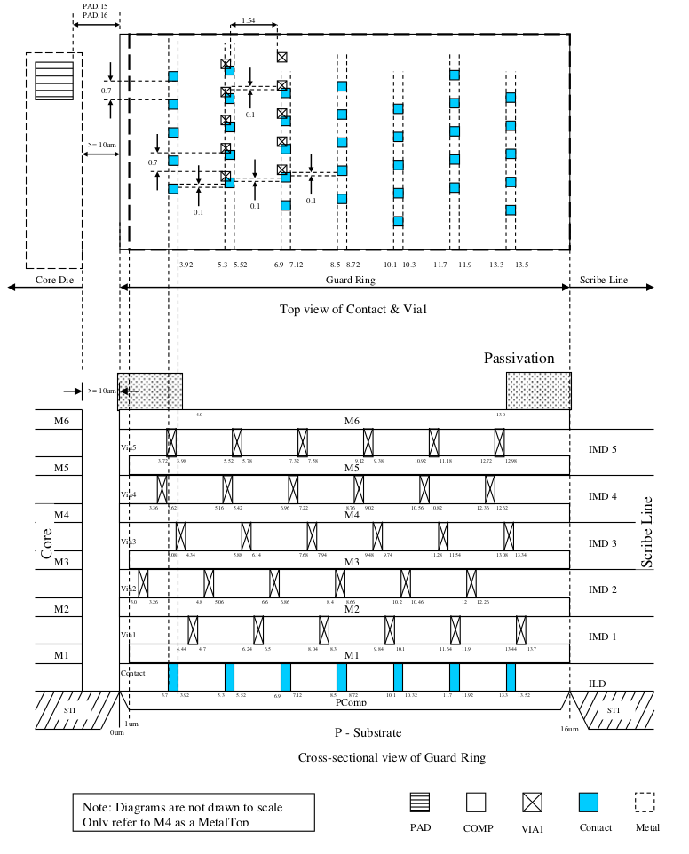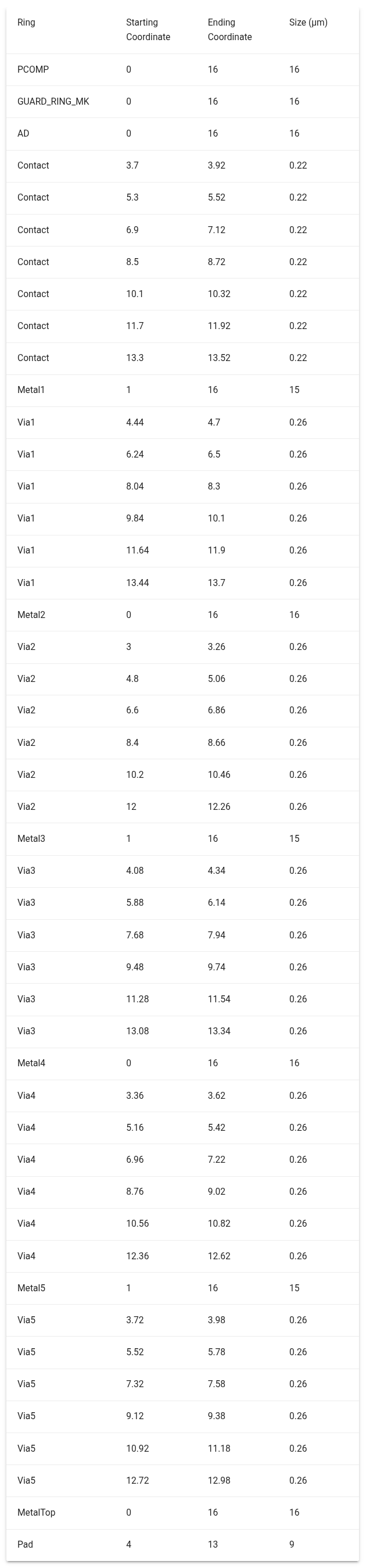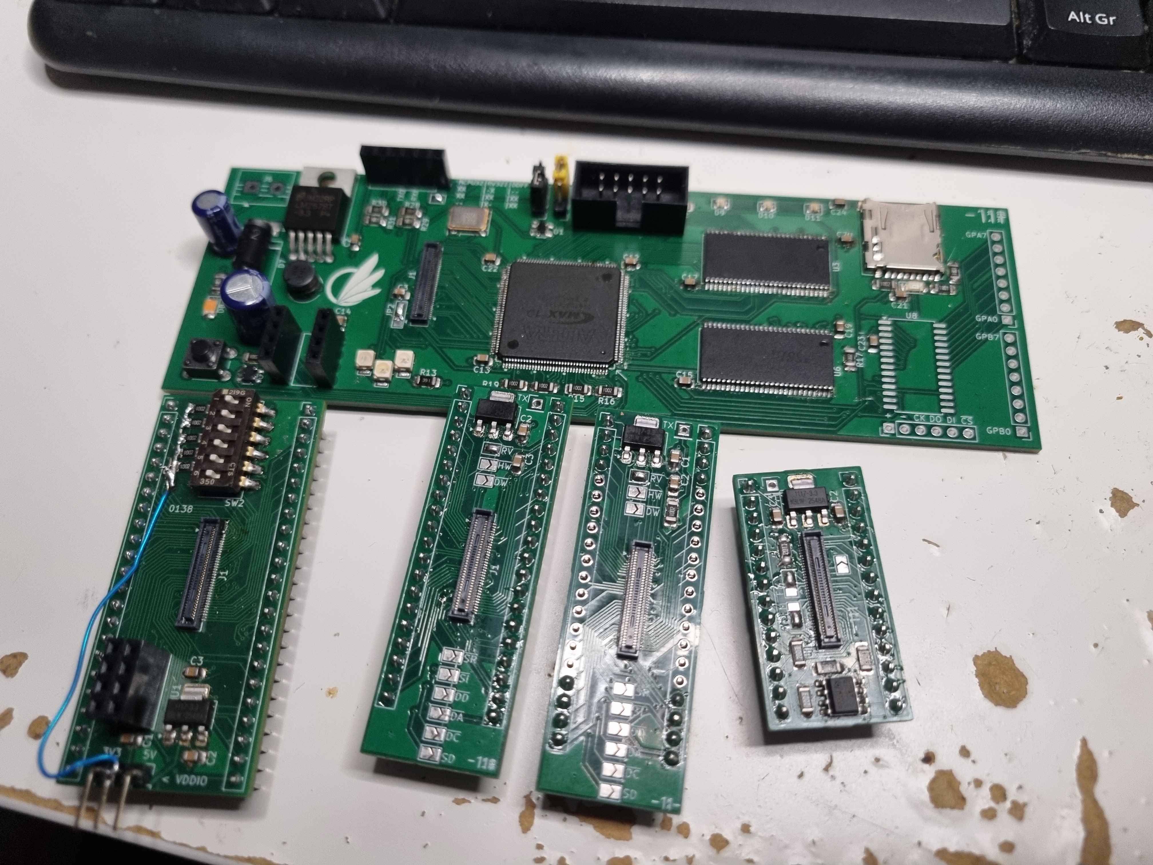
Guild icon
wafer.space Community
ℹ️ - Information / general
Welcome to wafer.space - documentation at wafer.space github - buy at buy.wafer.space - archives at discord.wafer.space
Between 2026-10-31 11:59 p.m. and 2026-12-01 12:00 a.m.

Avatar
Tim 'mithro' Ansell 2026-11-01 12:36 a.m.
NextPCB is likely the first
Avatar
Avatar
судонет
Not at all!
Tim 'mithro' Ansell 2026-11-01 12:53 a.m.
I think I saw from the shipping address you where in Sydney? I know a bunch of ASIC people in Sydney and UNSW has bought a slot on Run #3. I can do the introduction. (edited)
Avatar
Avatar
wafer.space Community #announcements
@everyone who ordered bare die from wafer.space Run #2 should have gotten a fedex tracking confirmation message yesterday for the shipment of the first ~200 bare die. If you haven't and think you should have, please poke me via email at tim@wafer.space I'm excited to see people bring up their projects! You can find out more about the various projects on Run #2 on the new pages @ https://wafer.space/ws-run2/ (edited)
Ah damn. I go on a short vacation or sorts starting on the 17th, so I’ll miss the initial COB shipment and my bring-ups will be delayed.
судонет started a thread. 2026-11-01 2:27 a.m.
Avatar
Avatar
Tim 'mithro' Ansell
NextPCB is likely the first
Ok, I saw pcbcart had just put a COB related blog post ( https://www.pcbcart.com/article/content/cob-wire-bonding-sensors.html ) so I thought this was related.
COB and wire bonding for sensor modules: bond selection, pull/shear tests, glob top, and DFM tips.
Avatar
Avatar
tnt
Ok, I saw pcbcart had just put a COB related blog post ( https://www.pcbcart.com/article/content/cob-wire-bonding-sensors.html ) so I thought this was related.
Tim 'mithro' Ansell 2026-11-01 10:29 a.m.
@stuart -^
Avatar
MCP4725-based addon for BondTest72 r2, providing a programmable LDO and precision 3.0V reference - namibj/BondTest72-Programmable-LDO
Avatar
Avatar
namibj
@Chips4Makers aka Staf Verhaegen could you please unbrick the build tooling for https://gitlab.com/Chips4Makers/arrakeen-sram-testchip/ , it seems you had written in a bunch of mentions of dev_SRAM branches strewn across the dependency web and it appears you've since deleted the branch which breaks uv. Notably, the mere uv run scripts/gen_views.py doesn't work and even trying to rewrite some of the lockfiles and even cloning and locally editing it's pyproject.toml of c4m-flexmem didn't suffice; next step would have been to clone and edit similarly PDKMaster to keep that as a dependency of c4m-flexmem from trying and failing to fetch @dev_SRAM of pdkmaster-io-spice.
Chips4Makers aka Staf Verhaegen 2026-11-01 11:33 a.m.
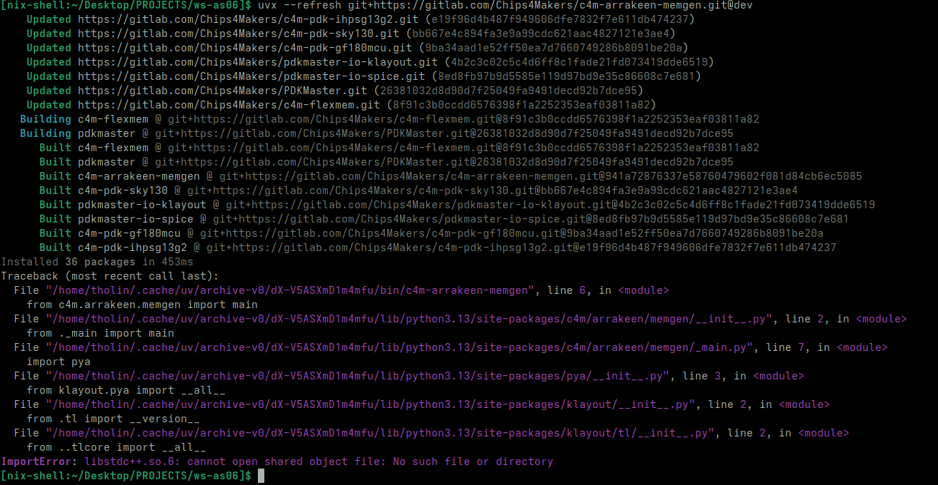
The latest dev branch should work. % uvx --refresh git+https://gitlab.com/Chips4Makers/c4m-arrakeen-memgen.git@dev This is project Arrakeen's memory generator. This is pre-alpha quality software; just above proof-of-concept level. Don't use it for production; no support is provided and use is at own risk! If it breaks you may keep the pieces. Select technologies: 1) IHP SG13G2 2) Sky130 3) GF180MCU ...
11:34 a.m.
512 is max. number of words currently supported by the compiler. The decoder generation for bigger number of words is not implemented yet.
Avatar
I'm gonna draw up a 2L flex board using the JLC special (5pcs up to 100x100 2L 1/3oz thin PI core only no stiffeners no soldering); I'm currently planning to do a multi-opportunity breakout board that utilizes the 3 flip chip bond pad structures in various combinations/styles (there's 3 nets; 2 of the 3 structures only have one pad per net; the third structure has larger grid pads and offers each net twice and routed so that it's at most diagonally/corner adjacent not sidways to challenge bonding processes that may be prone to shorting out adjacent pins), wiring out the DUT nets to some sort of "connector" that an ohmmeter can then be connected to for testing bond quality. What kind of connector would you think I should go with there? Some kinda 4-wire ZIF style replicated around the outer border to hopefully cover all the DUT bonds so that a tester could be ZIF-connected to all of them in series to try them? Just a wider ZIF connector for like each DUT/bond site approximately and plan on using an external breakout from that to a pin header or such? Solder connections for attaching pin headers to the flex around the edge after the flip chip bonding has been done? Any opinions? @Essen @Lauri @Andrew Wingate ?
Avatar
Primary testing would be 4-wire measurements of nets through the bonds at both ends; where applicable isolation testing is also on the docket. Where there are more than 2 pads for each net bonded out (there are 4 pads on the die for each net, but most DUT bonding sites on the test flex won't have all of them), the results from pairwise 4-wire measurements ought to reveal per-bond resistance, though possibly it might require adding a third voltage measurement wire into it, I'm not sure off the top of my head.
Avatar
Avatar
Chips4Makers aka Staf Verhaegen
The latest dev branch should work. % uvx --refresh git+https://gitlab.com/Chips4Makers/c4m-arrakeen-memgen.git@dev This is project Arrakeen's memory generator. This is pre-alpha quality software; just above proof-of-concept level. Don't use it for production; no support is provided and use is at own risk! If it breaks you may keep the pieces. Select technologies: 1) IHP SG13G2 2) Sky130 3) GF180MCU ...
yeah works. I took a look at the decoder generation code and it seems RowPreDecodersT could be taught to handle (address_groups[0] != 3), specifically, (address_groups[0] == 4), for a straight forward one extra bit (so up to 1024 words), as well as an easy extension by allowing to layer another pre-decoder in front of the current pre-decoder, where the new pre-decoder would merely act on this new (optional) 4th input bit of the current pre-decoder stage. It'd have to spread them a bit more vertically I think to not get routing congestion at the current last level decoder/page pitch, but otherwise I think it should work? And like, without having to make the row periphery wider. Unless this would not possibly fit in the limited routing channels on the left side over the input DFFs; it does look quite tight there. On further look it does appear to be mighty tight already.... Seems like it'd still be worth it though, at least with a word size notably larger than the tiny 8 bit (so that the extra decoder column of row periphery space doesn't dominate). @Tholin How large of an SRAM would you want to stick in that corner if you would get to wish anything the FlexMem compiler could support if it had sufficient demand to warrant the implementation/support effort?
Avatar
4096 x 8
4:51 p.m.
Actually, make that 8192 x 8
4:51 p.m.
If possible
4:51 p.m.
Idk if that’d fit
4:51 p.m.
I don’t even know if 4096 would fit
Avatar
Avatar
Tholin
I don’t even know if 4096 would fit
would you be happy with 512x64 with byte granularity write enable?
4:53 p.m.
single port, right?
Avatar
I'll generate the 512x64_8we first (oh, already done...), let's see how large it is.
Avatar
Avatar
Tholin
Yeah
can you measure me the area allowance?
Avatar
Avatar
namibj
would you be happy with 512x64 with byte granularity write enable?
this is 1102 wide and 246 tall
Avatar
Avatar
namibj
I'll generate the 512x64_8we first (oh, already done...), let's see how large it is.
2167 wide
Avatar
I can do 2167 by 246
Avatar
yeah the 512x64_8we should fit and actually you should be able to put 4 of them in horizontally I think.....
Avatar
Yep. Two of them, and I can do a version of the AS2650v2 that does not require caravel.
Avatar
the external column mux would be a "little" hard I fear
5:06 p.m.
well, density on it
5:08 p.m.
future works (inbuilt multiplexer/decoder support for getting more desiable aspect ratios despite narrow requested access bus width)
Avatar
What’s "uvx"?
Avatar
Avatar
Tholin
Yep. Two of them, and I can do a version of the AS2650v2 that does not require caravel.
due to the native width being "excessive", you could in theory even consider doing SECDEC ECC on it.... e.g. a 9th byte of width (72 instead of 64) is cheap there... the size would be in the coder, not the array.
Avatar
Avatar
Tholin
What’s "uvx"?
like npx but uv
5:10 p.m.
AFAIK
5:10 p.m.
you can also run from in the cloned repo
5:11 p.m.
if you ask what specific config I shall put in I can do it and send you a zip
Avatar
Avatar
Tholin
Click to see attachment 🖼️
welp 🙁 Feel free to tell me what config I'll generate it for you with the LEF and ngspice and verilog folders.
Avatar
It doesn't like the nix shell
Avatar
yeah I see
Avatar
Avatar
namibj
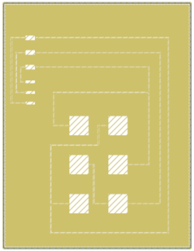
I'm gonna draw up a 2L flex board using the JLC special (5pcs up to 100x100 2L 1/3oz thin PI core only no stiffeners no soldering); I'm currently planning to do a multi-opportunity breakout board that utilizes the 3 flip chip bond pad structures in various combinations/styles (there's 3 nets; 2 of the 3 structures only have one pad per net; the third structure has larger grid pads and offers each net twice and routed so that it's at most diagonally/corner adjacent not sidways to challenge bonding processes that may be prone to shorting out adjacent pins), wiring out the DUT nets to some sort of "connector" that an ohmmeter can then be connected to for testing bond quality. What kind of connector would you think I should go with there? Some kinda 4-wire ZIF style replicated around the outer border to hopefully cover all the DUT bonds so that a tester could be ZIF-connected to all of them in series to try them? Just a wider ZIF connector for like each DUT/bond site approximately and plan on using an external breakout from that to a pin header or such? Solder connections for attaching pin headers to the flex around the edge after the flip chip bonding has been done? Any opinions? @Essen @Lauri @Andrew Wingate ?
@Tholin If you can, I'd appreciate some opinionated insight for the decision of how to "pin out" the group of flip chip DUT chips.
Avatar
The what?
5:21 p.m.
I’m not sure what useful input I could give on that
Avatar
The FC01 dies, I'm doing a 100x100 mm outline flex pcb with several footprint variants for this; to be tested and afterwards measured for bond resistance (you can see the traces somewhat on the die; those allow measuring continuity and also confirming that no adjacent pads got shorted out in the bonding process).

Avatar
Avatar
Tholin
I’m not sure what useful input I could give on that
I'm quite indecisive on the matter of 'what "connector footprint" to put around the edge(s) of the pcb to be convenient for subsequent measuring of whether the bonding attempts were successful'.
Avatar
I generated a 512x128 RAM and I believe I can fit it at the right hand side of the die
6:33 p.m.
Its actually almost a perfect fit height-wise
Avatar
Can’t get the RAM to hook up to the PDN for some reason
12:34 a.m.
I don’t think it likes being rotated 90 degrees
Avatar
Avatar
Tholin
Can’t get the RAM to hook up to the PDN for some reason
ensnare it in a macro power ring while rotated normally; then rotate it the 90 degrees?
Avatar
haha anyone have a microcontroller like chip on run 2?
Avatar
HZ80 plus DPK1 (the former Z80 clone bit banging firmware out of nonvolatile storage into the instruction memory of the bao IO controller thing (DPK1). ?

Avatar
Avatar
Paul
haha anyone have a microcontroller like chip on run 2?
wafer.space GF180MCU Run 2. Contribute to wafer-space/ws-run2 development by creating an account on GitHub.
Avatar
Avatar
Paul
haha anyone have a microcontroller like chip on run 2?
Andrew Wingate 2026-11-03 4:22 a.m.
@RebelMike has a number of them I believe.
Avatar
Avatar
Paul
haha anyone have a microcontroller like chip on run 2?
Yes, the run 2 version of TinyQV is along those lines: https://github.com/MichaelBell/ws02-tinyqv No dedicated I2C peripheral though potentially you could bit bang it (edited)
TinyQV for Wafer Space run 2 on gf180mcuD. Contribute to MichaelBell/ws02-tinyQV development by creating an account on GitHub.
4:38 p.m.
Does this chip not contain layouts created using my SCL?
4:38 p.m.
@Andrew Wingate
Avatar
Avatar
Tholin
Does this chip not contain layouts created using my SCL?
Andrew Wingate 2026-11-03 4:43 p.m.
Correct (I think) This was tiny tapeout's experimental chip. Maybe @tnt could give some better insight.
Avatar
Not usable ones.
4:47 p.m.
We had released the final GDS before the buf_8 fix so all the designs using that SCL are expected DOA.
Avatar
That’s not the case
4:47 p.m.
The buff_8 will still work, just with excessive power consumption when on (edited)
4:48 p.m.
One out of 8 transistors was shorted, and the remaining 7 are enough to power the short and still generate a clean logic level.
4:48 p.m.
Remember that this bug only got past me because the cell still passed SPICE simulation.
4:49 p.m.
(also its buff_8 not buf_8, I always hated the abbreviation of "buffer" with one "f")
Avatar
nice i'll talk to mike in DM's about it
Avatar
Were there also any RISC V micros in run 1 that people also have their hands on?
Avatar
I have a couple of TQVCs and have got them working
10:55 p.m.
TQVA-C are a straight port of the Tiny Tapeout design and so don't have full control over the IOs - the general purpose IO is split into 8 inputs and 8 outputs. That's fine for SPI but fairly terrible for I2C
Avatar
Magic has been taking a few hours on this one
11:49 p.m.
Is there a bug that it can get into an infinite loop?
11:51 p.m.
I think I found a bug
🤣 1
Avatar
Tim 'mithro' Ansell 2026-11-04 12:25 a.m.
https://wafer.space/ws-run2 is probably a nicer to view version
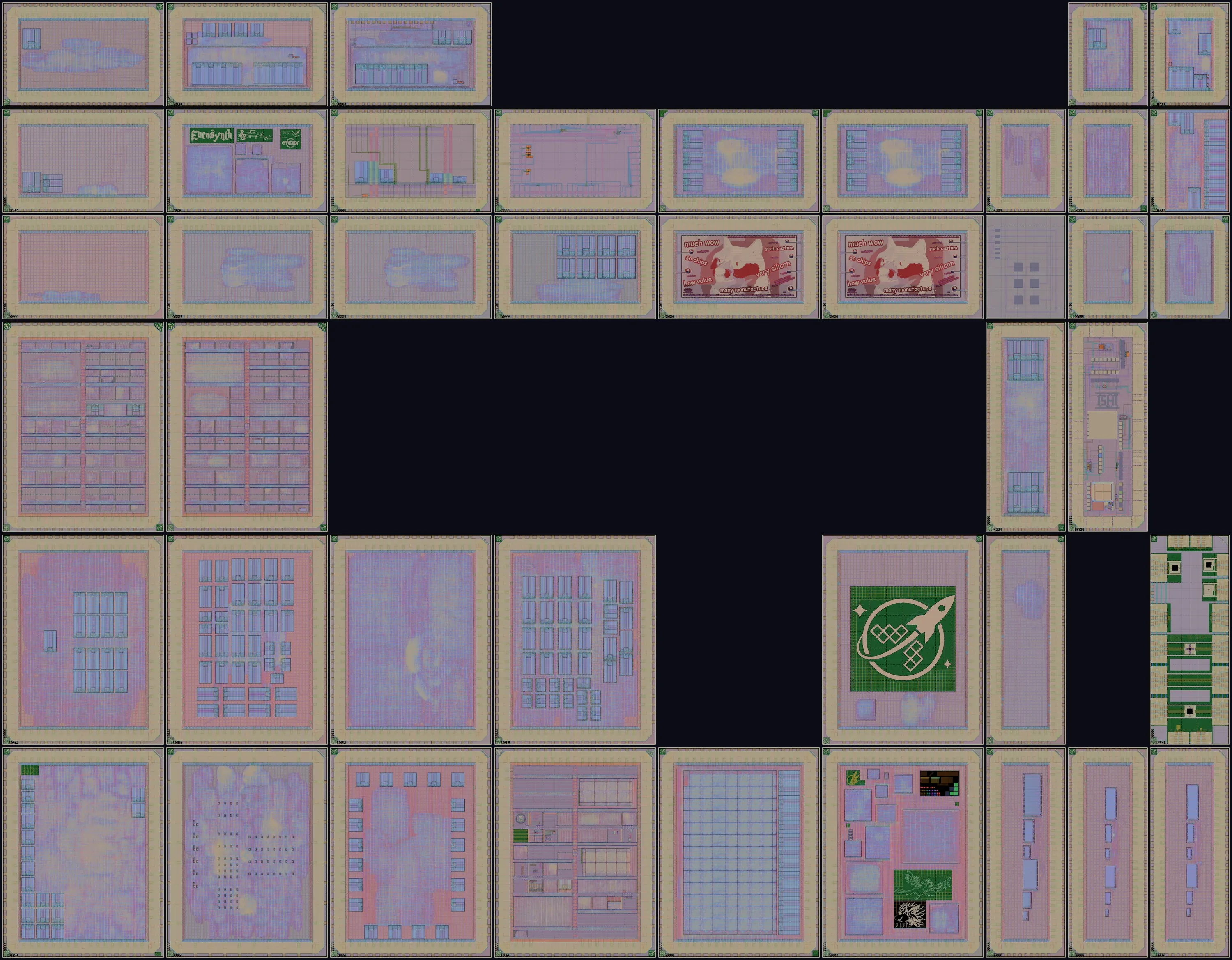
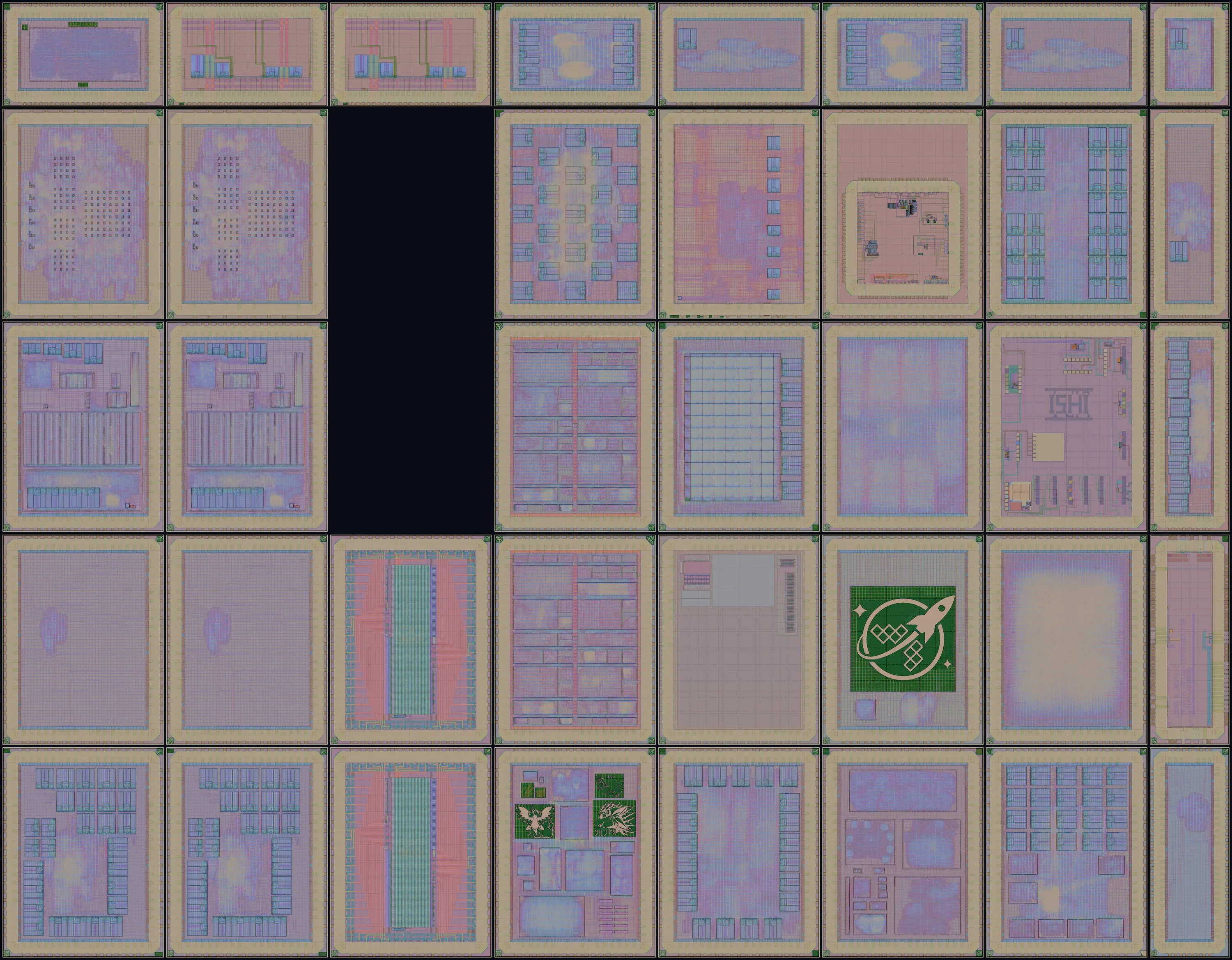
Designs, density statistics and layout renders from wafer.space GF180MCU Run 2.
❤️ 1
12:26 a.m.
Designs, density statistics and layout renders from wafer.space GF180MCU Run 2.
12:26 a.m.
Designs, density statistics and layout renders from wafer.space GF180MCU Run 1.
❤️ 1
Avatar
Getting a TON of antenna violations around the RAM now that it seems to be unable to repair
9:48 a.m.
Using this RAM generator has been a pain so far
👍 2
Avatar
Avatar
Tholin
Magic has been taking a few hours on this one
Chips4Makers aka Staf Verhaegen 2026-11-04 4:27 p.m.
Why do you need magic for LEF generation ? The compiler should also generate lef files.
Avatar
I modified the GDS file to have Metal4 strips for the PDN to contact
4:31 p.m.
I may have to edit it more. Getting lots of antenna violations still and what can usually help is moving the macro ports to a higher metal layer.
4:32 p.m.
I doubt I’ll be able to insert diodes inside the RAM, so I hope that’ll be enough.
Avatar
Ideally you wouldn't be editing the GDS but wrapping it.
Avatar
Chips4Makers aka Staf Verhaegen 2026-11-04 4:52 p.m.
Ideally OpenROAD should be able to handle the SRAM as is and do proper supply connection and antenna diode insertion. @Tholin Are you using librelane ? For my tape-outs @Leo Moser (mole99) helped me doing the tape-outs without needing to wrap the memory block. If I remember correctly for the half slot test chip the blocks were rotated also. It did contain minimal amount of logic though.
Avatar
I'm pretty sure it can. You need an appropriate pdngen configuration to tell it what to connect how.

Avatar
Idk how the Metal5 power straps could possibly connect to the RAM if it has no rails on Metal4
5:03 p.m.
And indeed the PDN did not make any connections until I added those
5:03 p.m.
But right now I’m more concerned about the antenna violations
Avatar
pdn gen is perfectly capable to connect down from Met5 to lower metal, adding island and via stacks as needed.
5:13 p.m.
But that's not something it will just do with default config.
Avatar
The generated LEF file is missing antenna information, maybe that’s why librelane is struggling to pick up on the antenna violations.
Avatar
Under normal circumstances, I’d do a LEF write from magic and have it generate this data, but it still gets stuck in an infinite loop when I try. (edited)
Avatar
Leo Moser (mole99) 2026-11-05 10:15 a.m.
@Tholin You can find the pdn setup here: https://gitlab.com/Chips4Makers/arrakeen-sram-testchip/-/blob/main/template/librelane/pdn/pdn_TestChip.tcl?ref_type=heads It's as simple as telling pdngen to connect Metal5 (PDN_HORIZONTAL_LAYER) and Metal3.
Avatar
I’m more concerned with the antenna errors
10:18 a.m.
I tried using insert ECO diodes to force diodes at all the RAM inputs and that made it worse
Avatar
Leo Moser (mole99) 2026-11-05 10:21 a.m.
You can load the .lyrdb file into KLayout to see exactly where and why antenna violations exist.


10:24 a.m.
Its all around the RAM
10:25 a.m.
The RAM generator does not put any antenna gate area information in the LEF.
10:25 a.m.
LibreLane doesn’t even pick up on the fact that there are these violations
Avatar
Leo Moser (mole99) 2026-11-05 10:34 a.m.
You could put some dummy antenna information in the LEF. And please open an issue at c4m-flexmem so Staf can keep it in mind.
A flexible, scalable memory generator.
Avatar
Avatar
Tholin
The RAM generator does not put any antenna gate area information in the LEF.
@Tholin different process, but this talks about adding diodes to sram inputs. https://discord.com/channels/1009193568256135208/1567679061235597363/1567898247991660565
Avatar
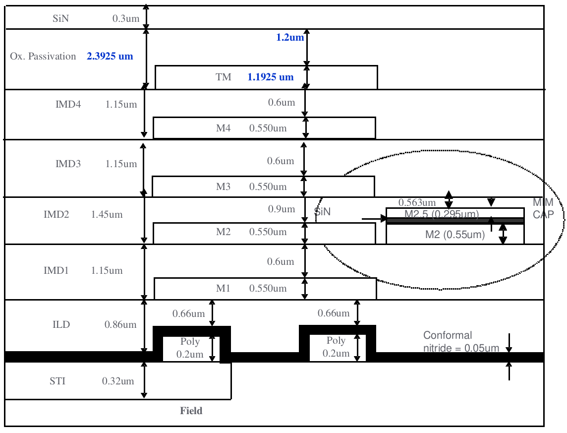
Hi! I’m planning a mixed-signal design for the upcoming GF180MCU run using the gf180mcu-project-template (gf180mcuD). Before I start the analog blocks, I’d like to confirm which optional process modules are included: MIM capacitor: Is MIM available on this run? If so, which option (1.0, 1.5 or 2.0 fF/µm²), and is it between Metal4 and Metal5 as in the Magic tech file? High-Rs poly resistor: Is the optional high-sheet-resistance poly (ppolyf_u_1k / _2k / _3k, mask L63) included, or should I stick to the standard unsalicided poly (ppolyf_u / npolyf_u)? Thanks a lot! Wenn du willst, kann ich die Frage noch kürzer oder förmlicher machen, etwa für eine E-Mail statt Discord.
Avatar
Avatar
InfoSecDJ
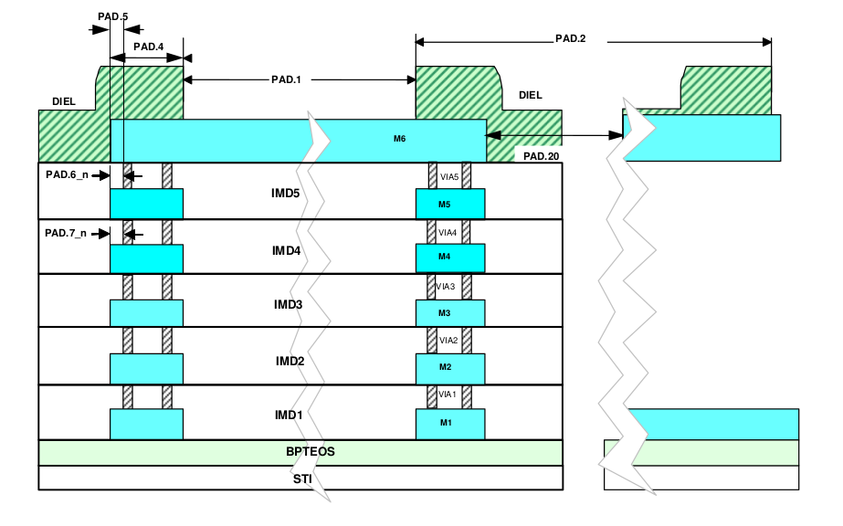
Did a cross-section through the pad.
Do we have any vaguely hard idea of the surface countour from a pad outwards? Or even in theory just around a pad?
Avatar
Avatar
namibj
Do we have any vaguely hard idea of the surface countour from a pad outwards? Or even in theory just around a pad?
@InfoSecDJ that cross-section you did through the pads, would it be difficult for you to apply some focus stacking or whatever necessary to get a good understanding of how the top surface actually looks from a topography POV? I'm asking to hopefully be able to pick an appropriate ACF tape that won't necessitate applying plating on the die to build the natural pad up into a true raised bump that reaches above the passivation's height.
Avatar
Avatar
namibj
@InfoSecDJ that cross-section you did through the pads, would it be difficult for you to apply some focus stacking or whatever necessary to get a good understanding of how the top surface actually looks from a topography POV? I'm asking to hopefully be able to pick an appropriate ACF tape that won't necessitate applying plating on the die to build the natural pad up into a true raised bump that reaches above the passivation's height.
the link below there is actually focus-stacked. see if that helps, and although passivation oxide is naturally invisible there, you can kinda infer where it ends -- that's where all the junk stuck in PI begins. looks quite a bit above the pad metal.
1:45 p.m.
🤷 at least that's how I interpret the visuals there, I might be wrong on that
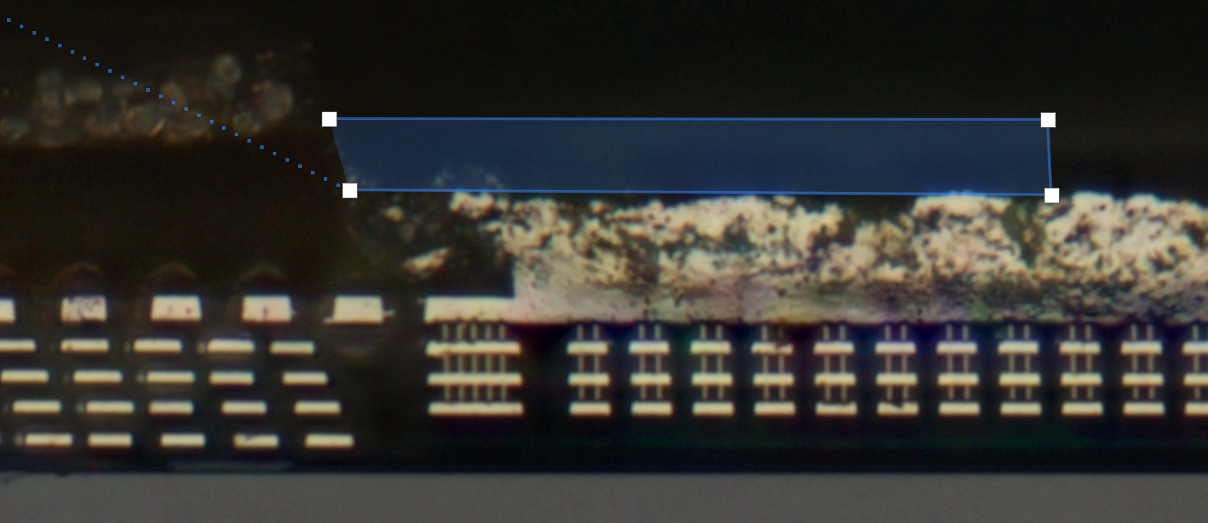
Avatar
Avatar
InfoSecDJ
the link below there is actually focus-stacked. see if that helps, and although passivation oxide is naturally invisible there, you can kinda infer where it ends -- that's where all the junk stuck in PI begins. looks quite a bit above the pad metal.
https://infosecdj.net/map/wafer-space/gf180mcu-ws1-xs1/infosecdj_nikpa100ncg/#x=11273&y=1053&z=6 Is it about this recess (I cut off the other side to the right to maintain this zoom level)?
Avatar
Avatar
InfoSecDJ
🤷 at least that's how I interpret the visuals there, I might be wrong on that
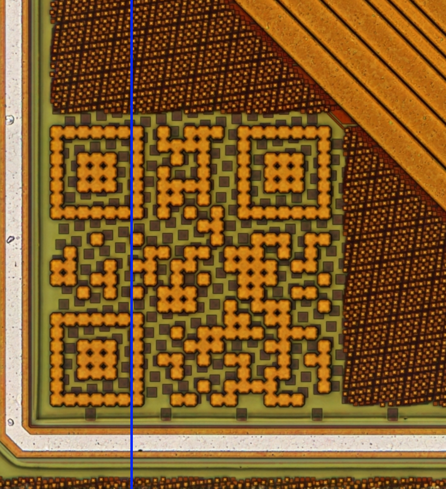
.....what direction to the pad frame was the image plane oriented, and while the die-thickness-reference and what's face of the die and what's backside-of-die are obvious, I'd like to have somewhat confirmed what's the right/left edge of the image region.
Avatar
On the right side is the corner of the pad frame. All the little square between the two pads are the fill pattern between the bond pads.
Avatar
Avatar
namibj
.....what direction to the pad frame was the image plane oriented, and while the die-thickness-reference and what's face of the die and what's backside-of-die are obvious, I'd like to have somewhat confirmed what's the right/left edge of the image region.
Avatar
Avatar
tnt
On the right side is the corner of the pad frame. All the little square between the two pads are the fill pattern between the bond pads.
If I measure at the right edge I do indeed measure that "pad opening" to be the DRC spec "wire bond"-class sealring's "pad opening".
2:09 p.m.
ahhh hmmm
2:12 p.m.
@tnt Do you think that perhaps using some polishing/flattening technique to get rid of the currently-raised ....polyimide? down to the height of the aluminium pads would work?
Avatar
Seems unlikely ... maybe some special solvant ...
Avatar
polyimide is, unfortunately, very resistant to solvents I know of. in fact, removing polyimide before imaging has proven to be a challenge for me here, as nothing I am able to obtain can do anything about it. so either heat or aggressive chem, neither of which is a good approach.
Avatar
Monoethanolamine ... good luck finding some 😅
Avatar
Avatar
tnt
Monoethanolamine ... good luck finding some 😅
does it actually work? is it worth the hassle of hunting for sources?
Avatar
Avatar
tnt
Seems unlikely ... maybe some special solvant ...
Oh I meant in a sense of planarization.
Avatar
Avatar
InfoSecDJ
does it actually work? is it worth the hassle of hunting for sources?
https://patentimages.storage.googleapis.com/57/b1/0f/1a678067b52dd4/US6319884B2.pdf Seems to work when mixed with some other one. There are dedicated solvants to it seems (made specifically for the Silicon industry), but those are probably harder to track down, although maybe @azonenberg knows where to get that kind of stuff ? (edited)
Avatar
In theory the easier treatment would be to run a zincate-ENIG plating though I don't think the "final" gold layer is as important for ACF tape as it is for soldering.
2:31 p.m.
I'm just rather poorly suited to do such properly, not alone because it sounds like it'd realistically involve nitric acid at around half of the regular non-fuming concentrate strength (i.e., 30 ish percent), and I recall concentrated nitric acid to be fairly regulated in and around Germany.
Avatar
you'd be very right on that.
Avatar
Concentrated sulfuric (at very elevated temps) or various oxygen/fluorine based plasmas are the usual options (edited)
Avatar
@azonenberg But wouldn't that attack the Aluminium too ?
Avatar
Not significantly, at least for the duration you need to get the polyimide off
2:42 p.m.
at least that's been my experience
2:43 p.m.
Backing up a bit: what is the overall goal?
2:43 p.m.
there will be overglass above the edge of the aluminum even if you remove the PI
Avatar
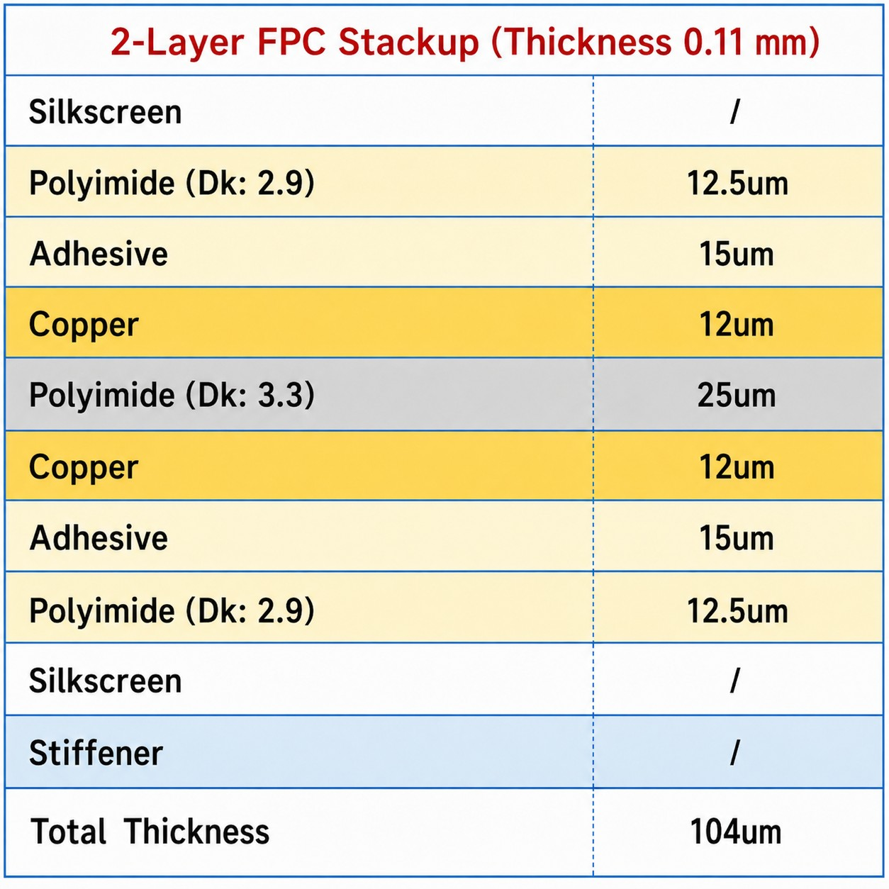
I guess there's hoping the pad thickness of around 4.5um and the passivation bump/buffer around it suffice to keep the 11um (c.f. stackup; the coverlay is pulled back around the relevant area anyways) copper traces that intersect the pads at the padframe and are otherwise aimed/oriented to escape from the die for now (there'll be tests to qualify an opportunity for future TinyTapeout to support direct pads over user tiles set up such that realistically a minimum analog project could hold 2 pads and an analog mux spine could sustain this, but there'd need to be probably at least one digital spine between two analog ones (vertical pitch) and if packing the die with this, there'd probably need to be two distinct flip-chip-fan-out setups where any given die can only support either the even-rows or the odd-rows of counting only analog spines).
Avatar
Avatar
azonenberg
Backing up a bit: what is the overall goal?
Do you know how ACF tape interacts with surface topography of both sides in a face-bonding application?
Avatar
how large are the filler particles in your tape?
2:45 p.m.
i would expect "normal" ACF to be far too large particles/pitch
2:47 p.m.
Like 3M 7303 is 43um particles and wants a 250um pitch
2:47 p.m.
which is far bigger than a bond pad
2:47 p.m.
i assume you can get smaller pitch stuff for COB/COF applications but i dont have specs for how much
Avatar
Avatar
azonenberg
how large are the filler particles in your tape?
I'm expecting "the fine stuff" that can realistically replace "classic" wafer level BGA-bumping for attaching to fine-pitch substrates. Like, the fine pitch stuffs that adapts from on the order of 100um pitch to 0.4~1mm BGA pitch as you may find in packages with multiple hundreds of balls.
Avatar
Avatar
azonenberg
i assume you can get smaller pitch stuff for COB/COF applications but i dont have specs for how much
https://www.resonac.com/products/semi-backend-process/77/001.html their AC-10000 series is Minimum contact area 3000 μm2 (which I incidentally match exactly) and MInimum Space 10 μm.
Resonac’s ACF connects film substrates, such as FPC and COF, to display panels. Resonac pioneered this film material that combines thermosetting resins and conductive particles to achieve both conductive and insulative properties.
Avatar
but no information on planarity requirement? does it list the sphere size?
Avatar
Avatar
azonenberg
but no information on planarity requirement? does it list the sphere size?
not directly, at least without "inquiry". As for planarity, well, it's generally a complex topic, due to how it interacts when manufacturing stuff.
Avatar
I had found a paper that did a test die they plated copper pillars onto and pushed face bonding rectangular array pad pitch substantially beyond what we could reasonably hope for on our stuff, at least without finding an MPW source for cheap silicon interposers or doing cursed stuff with face-to-face bonding of gf180mcuD dies (imagine face-bonding a half-height slot stuffed with SRAM and not having a bond pad ring, right over the core area of a full slot that otherwise gets "regular" COB wire bonding, to attach a comfy amount of fast RAM (very many pins possible, and no need for remotely bulky drivers due to inherently small capacitances) to something like a "normal" microcontroller or other general purpose ASIC). Edit: yeah, like maybe 128 kiB or a bit less could probably fit, I guess... (edited)
5:03 p.m.
I'll have to get outside and take care of some stuff while places are still open, and will see to grab the paper and whatever ACF nuances it iirc mentioned/detailed when I'm back home.
Avatar
Avatar
namibj
In this work, we present flip-chip hybridisation results combining Electroless Nickel Immersion Gold (ENIG) bumping with Anisotropic Conductive Film (ACF) bonding, both developed in-house. This method enables fine-pitch interconnections without requiring wafer-level processing.
ohhhh.... https://arxiv.org/abs/2511.15562 once again, CERN engineering boundary pushing drops off technology useful beyond CERN. With aligned-particle ACF they get down to 25um pitch.
@azonenberg here, the paper: they did 55μm pitch with the following:
The bumps obtained were 6 µm high above the pad, with a diameter of 19 µm. For the flip-chip hybridisation, an ACF of 18 µm thickness containing 3 µm-diameter nickel- coated conductive particles (CP) with a density of 71,200 CP/mm² was used. The ACF was laminated on the Ti-LGAD sensors at 90 °C under a pressure of 3.2 kgf (Fig. 1b), followed by bonding at 160 °C under 20 kgf for 2 s using a SET ACCµRA100 flip-chip bonder [7].
(edited)
5:31 p.m.
Excluding the weak center they attribute to vacuum grooves in the bonder head used (they could have done without the grooves but didn't have such a head ready/on hand), they got 99.5% well-connected bonds
5:42 p.m.
(for the record, we're aiming at like 30μm x 30μm pads at the small end, not 19μm diameter circles)
Avatar
DRC and Antenna clean
🔥 6
Avatar
Ready to receive my COBs
🔥 3
💯 2
💜 1
Avatar
Archit3ch (George) 2026-11-08 4:03 p.m.
has anyone tested their 3/2/1 sided pad rings from run 2? 🥺
Avatar
Avatar
Archit3ch (George)
has anyone tested their 3/2/1 sided pad rings from run 2? 🥺
I don't think anyone in the community has manufactured such padrings yet.
Avatar
Avatar
Essen
I don't think anyone in the community has manufactured such padrings yet.
Leo Moser (mole99) 2026-11-08 5:52 p.m.
Actually, LibreLane allows you to remove sides from the padring :) See Mike's TQVE: https://github.com/wafer-space/ws-run2
Avatar
I should make a motherboard for TQVD, and a CoB board for TQVE so we can test that out!
Avatar
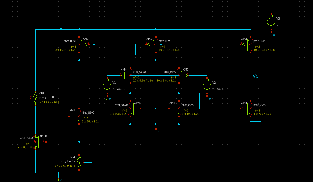
Can someone help me how layout this in Klayout please it would be pretty helpful. Thanks
Avatar
My friend and I are working on this project and have zero experience with Klayout. If anyone can help would be grateful.
Avatar
Avatar
alexp122
My friend and I are working on this project and have zero experience with Klayout. If anyone can help would be grateful.
This will not be the right community for getting help if you have zero experience. But the analog threads on Tiny Tapeout will be a better resource for you.
Avatar
Avatar
Essen
This will not be the right community for getting help if you have zero experience. But the analog threads on Tiny Tapeout will be a better resource for you.
Okey thank you for the help.
Avatar
You might want to check stability. A two stage op-amp without compensation could oscillate.
Avatar
Has anyone started testing of run#2 chips ?
👀 2
Avatar
Avatar
tnt
Has anyone started testing of run#2 chips ?
Andrew Wingate 2026-11-09 3:36 p.m.
Other than the small test we did, you are the first to receive any chips afaiu
4:25 p.m.
Is the COB being done for the others currently ?
Avatar
Avatar
tnt
😬
do tell what chips you got to try! ttgf0p3?
5:51 p.m.
(I thought that was a different COB base underneath?)
Avatar
Yes, ttgf0p3 assembled on a standard wafer.space breakout. Most TT chips will be bonded on a custom breakout that directly goes to our standard demo board, but the padframe is compatible with wafer.space COB so a few chips were mounted to it and I got a few samples.
Avatar
Avatar
tnt
Yes, ttgf0p3 assembled on a standard wafer.space breakout. Most TT chips will be bonded on a custom breakout that directly goes to our standard demo board, but the padframe is compatible with wafer.space COB so a few chips were mounted to it and I got a few samples.
ahhh I see. well, that LDO Add-On you AFAIK have gives you a fairly strong buffered DAC feed on COME if plugged in; it should suffice to e.g. read the ROM tile; unfortunately for this your reception of the gear was a surprise event to me; I didn't think anyone would actually have stuff they'd may wanna use the DAC Add-On for/with for at least the next several days.....
6:42 p.m.
oh reading helps; you've already connected it to a testbench driver setup of some sort given the reports made.
Avatar
I have a converter that allows me to connect those COB to the TT devboard, easier for testing 😅
👀 1
Avatar
Avatar
tnt
I have a converter that allows me to connect those COB to the TT devboard, easier for testing 😅
fair. I just checked and mathed some and I think the short of ua[1] to VSS on https://tinytapeout.com/chips/ttgf0p3/tt_um_mcml_vco could be electromigrated away over the course of hours to maybe a couple days (seems to mostly depend on how close to melting fuse in seconds one wants to push the trace).... Do you think the MUX will cope with some 10~40 (ish) mA into a fairly low resistance short to VSS (should be less than 5 Ohm I'd guess, at least for anything within the tile)?
Avatar
huh, out of 6 samples, I have 2 working ones, so I'm not trying anything crazy 😅
Avatar
oh no I wasn't suggesting you try anything like that with your precious frist wafer lot's first COB batch 😄
Avatar
also the thing has only 12 via3's to the VSS LEF pin :/
Avatar
I added a xor3 cell to my SCL, which was long overdue. This should help generate more efficient adders and thus improve the most common critical paths.
👏 1
Avatar
Avatar
tnt
Is the COB being done for the others currently ?
Yes, chips and boards are with the bond house now
Exported 180 message(s)
Timezone: UTC+0