I have not done that yet, but essentially from the research I've done you model the diode as a pulsed current source.
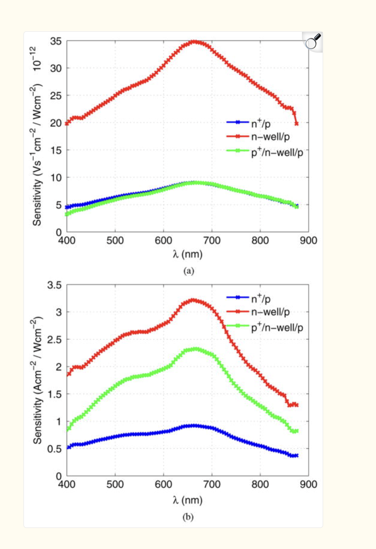
Where the current is I = Responsivity_curve * Light_intensity_in_watts/m^2 * Area of photodiode
While great advances have been made in optimizing fabrication process technologies for solid state image sensors, the need remains to be able to fabricate high quality photosensors in standard CMOS processes. The quality metrics depend on both the ...
8:16 p.m.
8:17 p.m.
I think the real answer is though unless you test it, it's all just fake numbers
8:17 p.m.
I think the amount of testing I want to do is just see how much signal I can get out at different magnitudes of current
makes sense, cheers for the details! excited to see this thing taped out
Do you have plans for packaging, or just setting it up on a prober for testing?
I'm not familiar enough with TCAD and what not. I don't know the answer
11:55 p.m.
@BreakingTaps I'm still trying to figure out how to package it. I really don't have much equipment to test anything. I would ideally like to do chip on board, but without the glue blob
1
11:55 p.m.
If you're interested or know anyone interested would love to work with people on making it happen
Will think on it! like 6 months ago I could have offered my shop services and a janky DIY wafer prober, but unfortunately I moved recently and am now shop-less




 Do you have plans for packaging, or just setting it up on a prober for testing?
 1
1