Guild icon
wafer.space Community
ℹ️ - Information / 📢-marketing
Channel for linking to "marketing" style content related to wafer.space - could include things like:
  • LinkedIn Posts
  • Twitter / Mastadon / BlueSky / other social links
  • Blog posts
  • News articles
Between 2026-09-30 11:59 p.m. and 2026-11-01 12:00 a.m.

Avatar
We’re looking for partners looking to develop cutting edge open source silicon with us, we’d like to do some codevelopment on our 10 purchased wafer.space slots
Avatar
What is the definition of "cutting edge" here? What exactly do you need?
Avatar
Analog characterization chip gigabit ethernet PCIE (any gen) Voltage regulators are top line items
Avatar
I can make you a linear regulator, but I don’t think the rest of those are possible
11:00 a.m.
Well, analog characterization depends on what you want to characterize
Avatar
Avatar
Paul
Analog characterization chip gigabit ethernet PCIE (any gen) Voltage regulators are top line items
All on a mature node of the late 1990s? You could have landed that money on a full GF180 MPW shuttle, if considering the minimum price you could have paid (~$20000, for 10x 0p5x0p5 bare die at early bird, which isn't even possible as there are just 9 of those), but you instead chose to buy 10 wafer.space slots where, even if you purchased at least a full slot, that 12.92mm^2 of silicon wouldn't handle most of the stuff mentioned. Other than potentially the linear voltage regulator Tholin mentioned.
Avatar
we’ve already invested the funds, and we have enough conviction to bet on something risky like this
11:48 a.m.
if it works, new possibilities on a mature 1990s node become possible
11:49 a.m.
we aren’t paying for engineering time, but we’re giving people a free shot at trying something risky, and if even 2/10 chips work, it’ll be a great success
Avatar
Avatar
Paul
if it works, new possibilities on a mature 1990s node become possible
The physics may disagree, sadly. Specifically transistor gate delays, and use of aluminium wire interconnects for the 5 metal layers.
Avatar
Avatar
Paul
we aren’t paying for engineering time, but we’re giving people a free shot at trying something risky, and if even 2/10 chips work, it’ll be a great success
It might be "giving people a free shot" in your perspective, but judging the "cutting edge tech" expected, it's still focus on a limited talent pool.
Avatar
100Mbit ethernet is in the spirit of the mission
11:56 a.m.
if you think these limits are too far out, then what do you think is possible? you of course have seen the 8086 demo scene
11:57 a.m.
the difference is that compiling code is free. well, we are making compiling silicon free
Avatar
Avatar
Paul
if you think these limits are too far out, then what do you think is possible? you of course have seen the 8086 demo scene
The 8086 demo scene was amazing because developers accepted the unforgiving hardware limits and optimised within them. They didn't try to force an 8086 MPU to render Crysis.
Avatar
Great, let's do that with GF180 then! DeepAI is looking for collaborators, chip designers, we're giving away 3 Run 3 slots in hope of pushing the boundaries of open source!
Avatar
Avatar
Paul
Great, let's do that with GF180 then! DeepAI is looking for collaborators, chip designers, we're giving away 3 Run 3 slots in hope of pushing the boundaries of open source!
I see! You donated one to Hack Club, right?
12:06 p.m.
I appreciate that gesture!
waferspace 2
Avatar
Even if you got those high speed interfaces on a gf180 chip, there is nothing you can put on that chip to generate or process data at those speeds.
12:26 p.m.
WCH makes a chip that is a PCIe to RS232 adapter (just a PCIe version of their popular USBTTL chips). If you put that on a board with a gf180mcu SoC and set it to one of the higher supported UART rates, i.e. 500000bps, you’d have all the throughput you need. (edited)
12:27 p.m.
To share my personal experience: I taped out a RISC-V core on GFMPW-1, about as performant as a non-pipelined core could get, and wired it up to a SPI <-> 10/100mbps ethernet bridge (enc28j60) and the system kept dropping packets because the RISC-V CPU struggled to process them faster than they were coming in. (edited)
12:29 p.m.
Like, it’d frequently die during IPv6 SLAAC or IPv4 DHCP because the broadcast responses combined with background broadcast traffic on my home network overflowed the buffer. (edited)
12:33 p.m.
So, 10/100mbps ethernet on gf180mcu would make sense, but then you’re hitting data processing speed limits anyways.
💜 1
Avatar
@Paul would you share any more specific or generalized goals you have in mind so we may better understand the landscape of what you may hope to achieve?
Avatar
I think aiming to increase the analog IP we have is your best bet here for producing something novel.
💯 1
12:38 p.m.
Analog on gf180mcu is still largely unexplored compared to the crazy things people are doing in sky130 TT analog slots now
12:39 p.m.
I believe there are also a lot of ways you can still make competitive products with analog, even on such an old process.
💜 1
💯 3
Avatar
Avatar
Tholin
I believe there are also a lot of ways you can still make competitive products with analog, even on such an old process.
Wholeheartedly agree. This thought also aligns somewhat with GF's general stance when deciding to stop pushing <12nm @Tholin can you share some ideas that are more specific? -# sorry my ignorance is showing
Avatar
My world view when it comes to analog is pretty narrow. I know people who do anything with music production equipment (i.e. synthesizer builders) would appreciate chips implementing the highly specific filter or VCO designs they need, with some mixed-signal processing sprinkled in for good measure. I know that a lot of analog oscillator and filter integrated circuitry operating on audio frequencies is very old designs from decades ago that may not even be in production anymore.
12:47 p.m.
Retro computing has a lot of mixed-signal sound and video generators that aren’t just VGA or a DSP + DAC.
💜 1
12:49 p.m.
I swear I had one more example on my mind, but I forgot while typing up the rest.
Avatar
It seems like this project's goals may be similar to Chipalooza, just intended to be on a grander scale. But the fact Chipalooza is also targeting this shuttle might mean some of the people with the required skills and free time to tackle these kind of problems are already busy. And some of the building blocks that will hopefully come out of Chipalooza would probably be useful for some of these more advanced goals (if gigabit ethernet/PCIE is even possible - high speed USB might be a more achievable goal?)
👍 1
Avatar
@Paul if you are interested and @Tholin is willing, I would be happy to help out integrating a SoC with Tholin's voltage regulator for one of the slots if that would be of interest. I wouldn't be able to do a self trimming oscillator as Tim suggested (though if anyone else here is available to do that I'd be happy to integrate it), but we could have something that was either driven from a ring oscillator or an external clock, with the ability to do USB CDC (traditional Full Speed only) if an external clock is supplied. We'd use the latest version of Tholin's standard cell library to prove that works as expected in a complex project. I haven't looked into Staf's SRAMs, but potentially we could use them as well, providing initial results from run 2 are positive. I've recently been working on an improved version of BIO - with more predictable instruction timing and improved instruction set over Baochip's BIO (https://www.crowdsupply.com/baochip/dabao/updates/bio-the-bao-i-o-co-processor), I don't know how usable that will be by the run 3 deadline but it would be cool to have the opportunity to tape it out even if it was a bit WIP.
BIO is the I/O co-processor in the Baochip-1x. In this update, I’ll talk about the origins of the BIO, starting by working through a detailed study of the Raspberry Pi PIO as a reference before diving into the architecture of the BIO.
Avatar
Considering my poor track record of first-trying analog design, please do not use my voltage regulator.
Avatar
Fair enough - I was just trying to get closer to the brief of a SoC that you can run with minimal external components. Maybe a SoC with the new cell library and SRAM is sufficiently interesting
Avatar
Avatar
RebelMike
@Paul if you are interested and @Tholin is willing, I would be happy to help out integrating a SoC with Tholin's voltage regulator for one of the slots if that would be of interest. I wouldn't be able to do a self trimming oscillator as Tim suggested (though if anyone else here is available to do that I'd be happy to integrate it), but we could have something that was either driven from a ring oscillator or an external clock, with the ability to do USB CDC (traditional Full Speed only) if an external clock is supplied. We'd use the latest version of Tholin's standard cell library to prove that works as expected in a complex project. I haven't looked into Staf's SRAMs, but potentially we could use them as well, providing initial results from run 2 are positive. I've recently been working on an improved version of BIO - with more predictable instruction timing and improved instruction set over Baochip's BIO (https://www.crowdsupply.com/baochip/dabao/updates/bio-the-bao-i-o-co-processor), I don't know how usable that will be by the run 3 deadline but it would be cool to have the opportunity to tape it out even if it was a bit WIP.
Andrew Wingate 2026-10-12 7:35 p.m.
I think the BIO is already on run2 This is it correct? https://github.com/dpks2003/bio-core
BIO Coprocessor on GF 180. Contribute to dpks2003/bio-core development by creating an account on GitHub.
Avatar
Yeah, that's basically a straight port of the Baochip version, and it doesn't have a host CPU. My aim is an improved version of BIO + either TinyQV or a more fully featured RISC-V core as the host.
💜 2
Avatar
@Andrew Wingate DeepAI is making it easier to gamble on open source silicon by giving out free silicon compilation to people pushing the boundaries. That's why we got the 10 slots. Our own project is developing a new ai agentic cpu architecture, and we're starting small. We just think custom silicon should be as plentiful and as easy to make as opens source code
12:38 a.m.
High speed interfaces are an interest of @baragonaru, who's the lead designer of Chippy, the ai agent CPU. We're also following the guidance of @Tim 'mithro' Ansell on what projects would help open source silicon the most, along with a few advisors and friends, like in this thread
12:39 a.m.
Like what was said earlier, analog work is something that is feasible and is lacking on the open source end. Projects like the voltage regulator or the calibration chip are along this line
12:40 a.m.
@Tholin yes, let's do the regulator. Do you want to fit it inside the analog calibration chip? Could be interesting way of testing and getting some instrumental value out of it
12:41 a.m.
@RebelMike sure, we want to do something with RISC-V this run, could you DM me with your 1 pager on the chip?
Avatar
Andrew Wingate 2026-10-13 7:10 a.m.
@RebelMike, @bunnie has seen you were working on BIO improvements https://discord.com/channels/1361349522684510449/1413281558407942236/1559267339713642547 and is interested in reading/seeing more if you have anything.
Avatar
I should write something up 😄
😂 1
Avatar
I don’t think I’ve even pushed the repo to GitHub yet. But the main things I’ve done: Use FemtoRV as the core. 2 clocks per instruction for all instructions except memory access and branches. Predictable performance in general to allow cycle counting. No C extension. Add some B extension instructions. In particular I found rotates being missing a problem when writing for BIO as it meant you couldn’t easily shift bits out to an arbitrary pin. Bit and byte reverse. And the logical ops with one inverted operand.
👍 1
Avatar
One note, so far this is a rewrite. I haven’t been referencing the original BIO implementation, just the spec. But also I haven’t got as far as doing the FIFOs yet - I’ve just got GPIO working on a single core. So possibly this would be a good point to try and transplant what I have into the original BIO implementation, especially if this project might be gaining a deadline.
💜 1
Avatar
Avatar
RebelMike
One note, so far this is a rewrite. I haven’t been referencing the original BIO implementation, just the spec. But also I haven’t got as far as doing the FIFOs yet - I’ve just got GPIO working on a single core. So possibly this would be a good point to try and transplant what I have into the original BIO implementation, especially if this project might be gaining a deadline.
Andrew Wingate 2026-10-13 7:55 a.m.
I guess @bunnie is somewhere that blocks discord
Ah that's pretty nice to have the B extensions. Are these specifiable as a standard compiler option or will this require hand coded assembly? Lol I had the theory that you would not want to cycle count because you can rtl simulate, but it's not a bad idea to shorten the pipeline regardless The C instructions are sort of important actually for both fetch bandwidth and instruction density. 4k is very small I was contemplating a next gen for bio, so this is useful. Actually a test bench is really valuable, I would like to copy any test code he has and add it to the tests, and maybe start a CI if there is actually interest in developing the BIO
7:57 a.m.
Not sure if he is interested in collaborative work tho or if he would prefer just to dev on a branch and then I cherry pick whatever I want for a next tape out I would like to roughly double the performance of bio by the next gen
~ bunnie
Avatar
I'm finally out of that region. For whatever reason, Turkey hates Discord. Thanks for tunneling the messages @Andrew Wingate !
💜 1
Avatar
Avatar
bunnie
I'm finally out of that region. For whatever reason, Turkey hates Discord. Thanks for tunneling the messages @Andrew Wingate !
судонет 2026-10-13 9:38 a.m.
yeah, heard some crazy stuff happened there that caused it
😱 1
Avatar
I would love to talk more about the BIO stuff - not sure if wafer.space would like us taking over the marketing channel for a deeper technical discussion, how would you feel about continuing the discussion over on the Baochip discord in the #bao1x-chip channel?
Avatar
Avatar
судонет
yeah, heard some crazy stuff happened there that caused it
oh...wow...ok yah I just googled it. I won't repeat here because O/T but dang. I couldn't tell if it was the hotel I was in or Turkey as a whole this confirms Turkey-wide ban.
Avatar
DM’d you guys both @RebelMike @Tholin
👍 1
10:34 a.m.
and @судонет
👍 1
10:34 a.m.
Calling all brave souls!
Avatar
Avatar
bunnie
I would love to talk more about the BIO stuff - not sure if wafer.space would like us taking over the marketing channel for a deeper technical discussion, how would you feel about continuing the discussion over on the Baochip discord in the #bao1x-chip channel?
Sure - I'm busy today but will do this evening! And yeah, this got quite off topic for this channel 😆
❤️ 1
Avatar
Avatar
RebelMike
@Paul if you are interested and @Tholin is willing, I would be happy to help out integrating a SoC with Tholin's voltage regulator for one of the slots if that would be of interest. I wouldn't be able to do a self trimming oscillator as Tim suggested (though if anyone else here is available to do that I'd be happy to integrate it), but we could have something that was either driven from a ring oscillator or an external clock, with the ability to do USB CDC (traditional Full Speed only) if an external clock is supplied. We'd use the latest version of Tholin's standard cell library to prove that works as expected in a complex project. I haven't looked into Staf's SRAMs, but potentially we could use them as well, providing initial results from run 2 are positive. I've recently been working on an improved version of BIO - with more predictable instruction timing and improved instruction set over Baochip's BIO (https://www.crowdsupply.com/baochip/dabao/updates/bio-the-bao-i-o-co-processor), I don't know how usable that will be by the run 3 deadline but it would be cool to have the opportunity to tape it out even if it was a bit WIP.
I characterized my voltage regulator a little more. The maximum current it can handle while supplying a usable voltage is between 100 and 150mA, so you’d be on a tight power budget.
Avatar
I can make a version that can push 450mA if the supply voltage is at least 5V, but you’re on your own for integrating it into LibreLane
Avatar
Avatar
Tholin
I can make a version that can push 450mA if the supply voltage is at least 5V, but you’re on your own for integrating it into LibreLane
Out of curiosity, what about that version would LibreLane not like? Are the features too large or something?
Avatar
I mean, how you’d get it to interface with the PDN correctly?
11:37 a.m.
Its a macro that both takes in a supply voltage and outputs another supply voltage (edited)
💜 1
Avatar
we’re opening up our slots to any good, kinda crazy ideas now! Big points if two or more decide to go in on the same project!
🤣 2
Avatar
Avatar
Paul
we’re opening up our slots to any good, kinda crazy ideas now! Big points if two or more decide to go in on the same project!
A friend of mine plans to design a 16-core 32-bit CPU of custom ISA for some reason. He's crazy!
🔥 1
Avatar
Avatar
RebelMike
Sure - I'm busy today but will do this evening! And yeah, this got quite off topic for this channel 😆
Tim 'mithro' Ansell 2026-10-14 10:48 p.m.
I'm happy for BIO related discussions to happen on the wafer.space discord (as I'll be able ot see them then :-), I can even create you a channel if you want?
Avatar
Avatar
судонет
A friend of mine plans to design a 16-core 32-bit CPU of custom ISA for some reason. He's crazy!
do you think you and your friend could join forces on a slot?
👍 1
Avatar
Avatar
Paul
do you think you and your friend could join forces on a slot?
Absolutely.
12:30 p.m.
He's in on the idea.
Avatar
@Tim Edwards I was just chatting to @Paul about their plans to sponsor silicon on run 3, and it seems like their goals to help develop open source silicon overlap quite a bit with Chipalooza. It might be worth you guys getting in touch! Paul - for reference the details of the Chipalooza challenges are here: https://opencircuitdesign.com/chipalooza/index.html
💜 2
Avatar
@Tim Edwards hi hi!
3:52 p.m.
DM sent, thanks Mike!
Avatar
Avatar
Paul
@Tim Edwards hi hi!
If you sent a DM to me, I didn't get it, but I'd love to chat about this.
💜 1
Avatar
1/4 slot free for analog work! @Tholin ‘s fabbing out on a slot of ours and she has 1/4 space left! We’re interested in an analog calibration chip, something that uses her IP to validate analog properties of the process and develop a physics simulator.
12:08 p.m.
  • 46 bi-directional IOs
    • Separate core/IO voltage with the level-shifting IO pads
    • 4 analog outputs using 12-bit DACs
    • Dedicated clock pad
Avatar
Those specs are for digital
12:12 p.m.
If you’re going to do analog in that space, you’ll have to put probe pads of your own in there
Avatar
looking for someone to help out @namibj ‘s collaboration with @Tholin with librelane scripting!
Avatar
Avatar
Paul
looking for someone to help out @namibj ‘s collaboration with @Tholin with librelane scripting!
basically, get librelane to PnR an analog crossbar-ish switch matrix that can select a parametric number of columns to be connected to available shared rows; set up for a digital decoder to trigger the entire column group together once "that specific DUT" is selected out of all there are, and at least somewhat deal with placing DUTs in an area-economic packing arrangement on the side of the switch matrix. And wire/auto-route from the responsible switch columns up to the DUT's declared "pads" ("LEF pins"). I'll be able to help with pretty much anything on it, I just don't have enough days of "flow state in the zone" coding to schedule for/on it until the deadline to do it alone.
Avatar
@судонет ?
Avatar
@brookieoz would you be interested in advising on this project? and perhaps @судонет and his friend would be interested in doing the implementation?
Avatar
Avatar
Paul
@brookieoz would you be interested in advising on this project? and perhaps @судонет and his friend would be interested in doing the implementation?
@Agenxy may also have some pertinent suggestions (once things are further along; there's some primitive devices I really want models for and the SCL stuff can wait until there's time left and the primitives are succesfully PnR'd) on affordably-enough-in-area-overhead and with enough ability to calibrate out muxing harnesses: ways to also measure DUT capacitances as needed for modeling AC behavior, not just DC operating points as the plain "muxed e-test" (with kelvin connections to calibrate out the MUX resistance) does. (Personally I'm not so sure that needs measuring by us like this, but idk for sure. I'd expect the existing RLC e-test structures on iirc Run2 can sufficciently de-embed muxing-tolerant RLC measurement tactics that can affordable provide detailed statistical distribution data, with which then model/extraction fit tuning could be done using the measured DC op point behavior to find SPICE model fits of parasitics that together with the known statistics of DC behavior of DUTs can accurately explain compound-DUT-arrangements behavior under AC conditions.)
Avatar
maybe? I haven't kept up with what's going on; just been so busy. How in depth are we looking to characterize things?
Avatar
Avatar
brookieoz
maybe? I haven't kept up with what's going on; just been so busy. How in depth are we looking to characterize things?
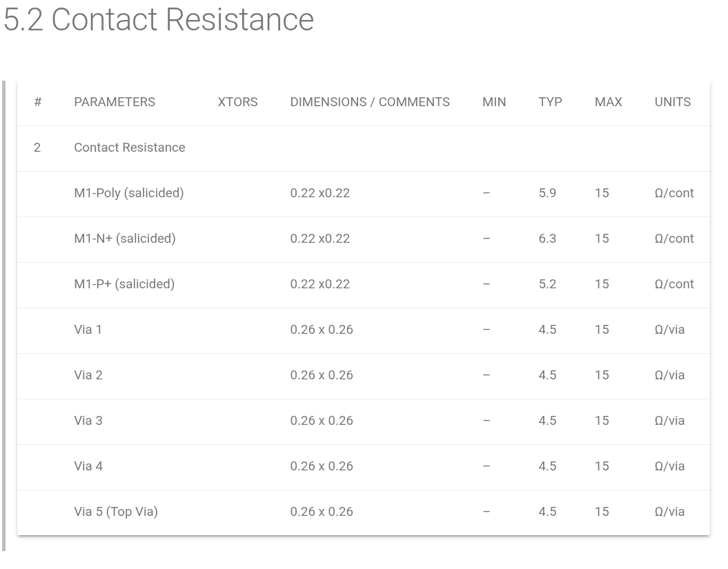
the base "muxed e-test" is just an analog switch matrix on the same die as a bunch of DUTs; a simple digital decoder selects one DUT, activates those switches and deactivates the others; there's two wires to each DUT "LEF pin"; off-chip multimeters are then scripted/remote-controlled to sample a few hundred/thousand "interesting" bias conditions of the DUT; then the mux is changed to select the next DUT; then this repeats; after a few minutes the setup rings a bell/buzzer/status-light and a nearby human swaps in the next COB at convenience; this allows measuring hundreds of dies under DC operating point conditions without very expensive raw wafer probe stations. Might repeat it afterwards with the test chip and it's socket-board in a freezer and/or oven or if thermal mass works out small enough a 2/3 stage peltier chamber might even give the essentially-full specification range of die temperatures without being a genuinely expensive chamber and without the human having to touch each chip once for each temperature. The big things are just that thin oxide nvt NMOS have zero SPICE and zero e-test data (at least NDA-free), a bunch of stuff has zero local mismatch statistical models, that latter includes (notably!) plain vias which promise a factor of over 3 from typ to max and no min (breaks predictable matching of differential pair resistor divider kind-of structures, without spending a bunch of space and parasticic capacitance on spamming vias in hopes of the unspecified statistics being the type that's persuaded by such tricks).
6:53 p.m.
You probably don't have to do much tho. I'd likely just ask occassionally for some wisdom on some concept/larger decisions that exceed what I can handle with intuition and where precision isn't worth setting up enough SPICE testbench to "ask the models" for guidance.
Avatar
oh yeah testing NVT devices is a little bit tricky since you typically can't just tie the source to GND / you want to be able to control the source voltage while measuring the current
Avatar
Avatar
brookieoz
oh yeah testing NVT devices is a little bit tricky since you typically can't just tie the source to GND / you want to be able to control the source voltage while measuring the current
....place the mux array in a dnwell? run negative bias to the lvpwell's inside that?
7:05 p.m.
but I don't think it really has to be measured accurately over exotic voltages anyways, and not all measurement bias conditions have to come from the very same DUT even if they are the same dimensions; e.g. a DUT could have a source diffusion very hard tied to a low impedance GND to handle substantial current on it if so desired. Not like similar situations don't affect many regular nmos DUTs.
Avatar
It's mostly that I see NVT devices being used as cascodes or input pairs or other things (common gate amps, etc) where you definitely don't have source connected to GND and where you do somewhat care about body effect / gate coupling factors
8:20 p.m.
so having a model that accurately captures that would greatly benefit any designs that use the NVT devices
Avatar
Avatar
namibj
....place the mux array in a dnwell? run negative bias to the lvpwell's inside that?
Running a negative bias to the lvpwell is going to be a little difficult if you're putting them through a mux that uses NMOS's if those NMOS bodies are tied to GND
Avatar
Avatar
brookieoz
Running a negative bias to the lvpwell is going to be a little difficult if you're putting them through a mux that uses NMOS's if those NMOS bodies are tied to GND
No I meant the mux itself sits in a dnwell and uses local lvpwells to provide a negative body to the transmission gate's nmos parts. Coughing up that negative bias could worst case be done with a charge pump but tbf the concept would need analog IO pads that can carry a negative signal voltage w.r.t. substrate anyways.
Avatar
Avatar
brookieoz
It's mostly that I see NVT devices being used as cascodes or input pairs or other things (common gate amps, etc) where you definitely don't have source connected to GND and where you do somewhat care about body effect / gate coupling factors
Yeah wouldn't all nodes of a thin oxide one be fully between 0V and 5V then, with substrate tied to 0V?
Avatar
Avatar
brookieoz
🤔
Needs adapted ESD structures to not have a clamp diode to substrate but that can't be hard.
Avatar
To be honest if I can avoid it, i'd rather just not deal with negative body biasing and just be able to sweep Vs and Vg independently (with Vd connected to supply or another independent thing)
Avatar
(the only reason to need a negative lvpwell in the mux tgate is to switch signals below 0V, and one end of those switches is low impedance connected to a wire bond)
Avatar
Avatar
brookieoz
To be honest if I can avoid it, i'd rather just not deal with negative body biasing and just be able to sweep Vs and Vg independently (with Vd connected to supply or another independent thing)
It's a 3 terminal device, plus substrate; you get 7 wires muxed to it: a substrate sense wire and a kelvin pair for each of source/drain/gate.
Avatar
Oh neat
Avatar
Avatar
brookieoz
Oh neat
I thought you wanted to apply negative gate at near zero source and drain because they PVT a threshold of like 50 +-300 mV or such.
Avatar
Oh nahh
8:57 p.m.
What I would do is apply a negative VGS but the actual values of Vg and Vs can still be positive, just that Vs can be greater than Vg
8:58 p.m.
So like, a Vg of 0.5V but a Vs sweep from 0->1.8V or something like that
8:59 p.m.
and to characterize the gate coupling factor you'd need to do a Vs sweep at different Vg's
8:59 p.m.
That kinda thing
Avatar
That's the power of the mux. The full large one can do that to an entire SCL oai33
🩵 1
Avatar
Avatar
brookieoz
and to characterize the gate coupling factor you'd need to do a Vs sweep at different Vg's
The task is to calibrate an e.g. PSP103 SPICE model card.
Avatar
Avatar
namibj
That's the power of the mux. The full large one can do that to an entire SCL oai33
That's 17 wires (GND sense, power (x2), output (x2), 6 inputs (x2))
Avatar
@namibj late reply on capacitance through the mux, and I'm more of a digital person, so take it with salt: the approach I've seen for small caps with only DC access is charge-based capacitance measurement (CBCM). You clock two matched tiny inverters, one with the DUT as its load, and the difference in average supply current gives you C. Might be worth a look. Still happy to share my corner data if it's useful.
Avatar
hey @Tholin @namibj have you guys talked yet?
9:25 p.m.
and @судонет
Avatar
No. I’m just waiting to be handed a GDSII.
Avatar
Avatar
Agenxy
@namibj late reply on capacitance through the mux, and I'm more of a digital person, so take it with salt: the approach I've seen for small caps with only DC access is charge-based capacitance measurement (CBCM). You clock two matched tiny inverters, one with the DUT as its load, and the difference in average supply current gives you C. Might be worth a look. Still happy to share my corner data if it's useful.
that's a good idea, charge-based not caring about supply resistance like that
Avatar
Avatar
Agenxy
@namibj late reply on capacitance through the mux, and I'm more of a digital person, so take it with salt: the approach I've seen for small caps with only DC access is charge-based capacitance measurement (CBCM). You clock two matched tiny inverters, one with the DUT as its load, and the difference in average supply current gives you C. Might be worth a look. Still happy to share my corner data if it's useful.
Ok, so, I don't think it would work to have a single DUT wired to both analog MUX with split sense/drive wires to each of it's pins and also fit a tiny inverter powered from a measurable/sufficiently-muxed supply connected to that very same DUT, because that'd be trying to measure the analog MUX's capacitance summed with the DUT pin's capacitance, right?
Exported 115 message(s)
Timezone: UTC+0