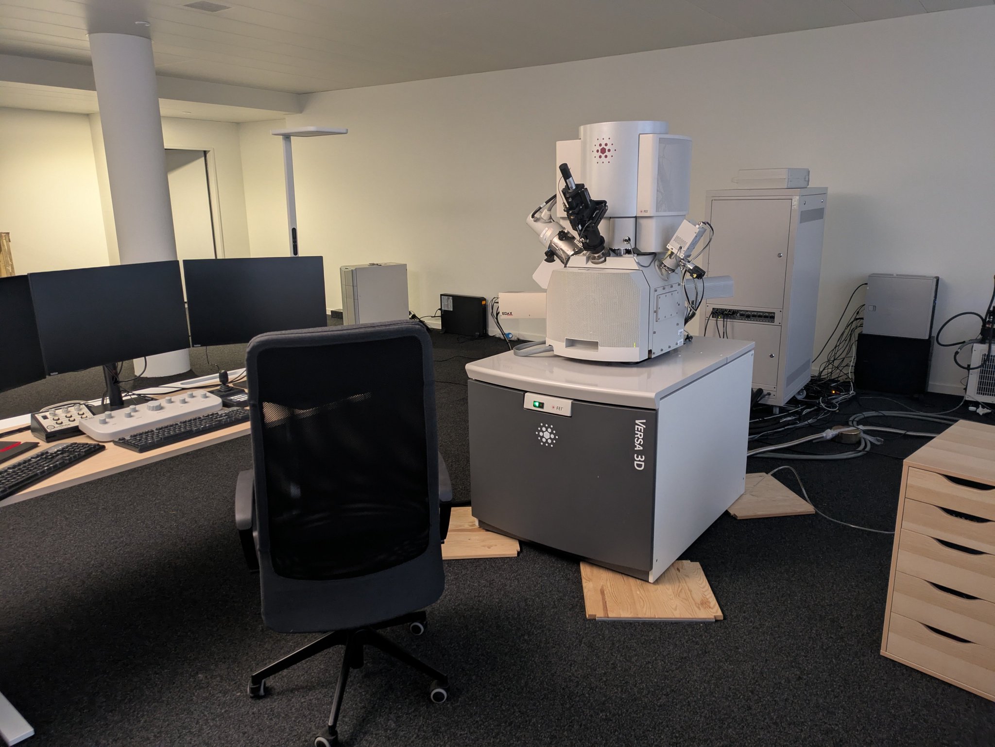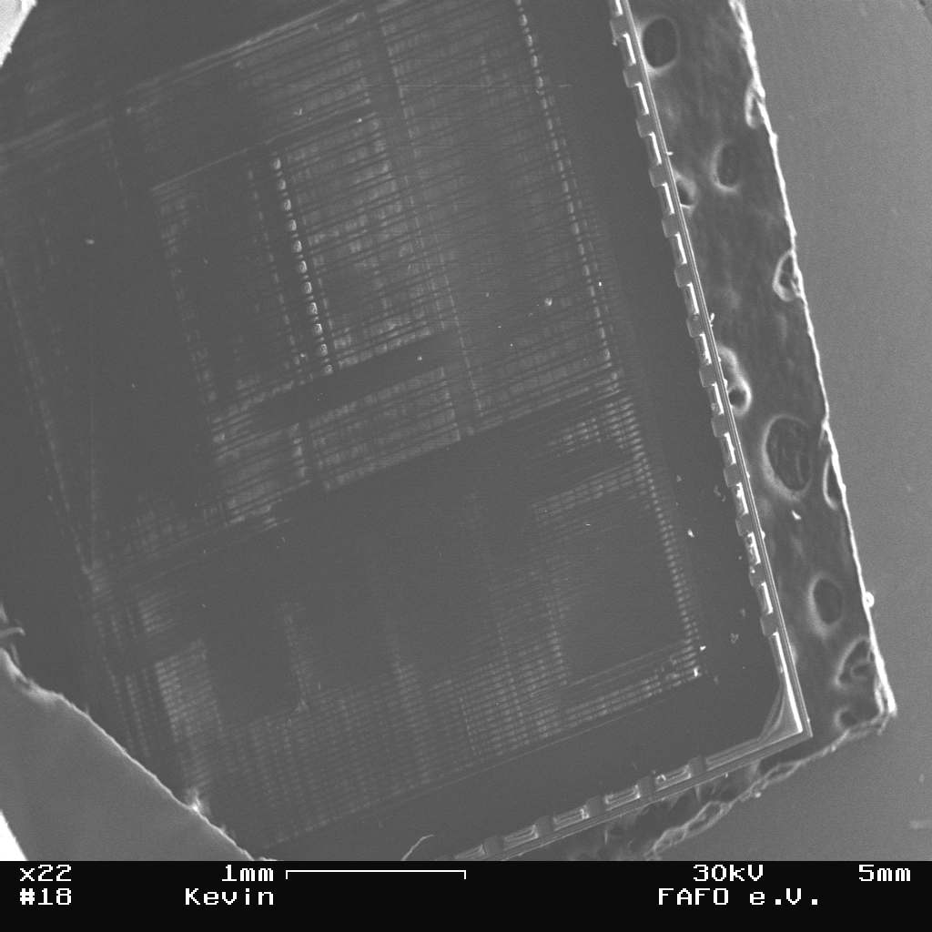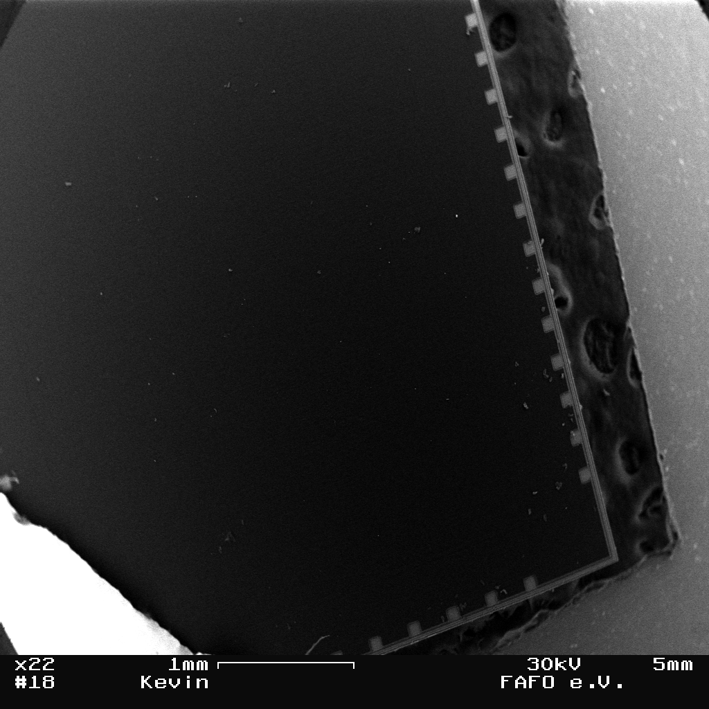
Hey there! Hope this is the right place to ask, got directed here by Matt. I threw an efabless OpenMPW GF180 die under the SEM today (not sure which shuttle this was, I was gifted this by a friend who wanted to get some SEM shots of it). Did not do any prep to the die other than cleaning, expected to see the topmost metal layer across whatever passivation later might be on top, same as with the SKY130 dies from an earlier OpenMPW run. However, the die was fully opaque to BSE and only very light contours of... CMP pads? Maybe PDN? were visible with SE imaging. Even at 30kV! Is this just that GF180 has one damn thick passivation layer on top, or am I missing something?
First photo is SE, second is BSE.
(The bright thing in the bottom left corner is copper tape for better sample conductivity. I cannot promise that this is standard procedure for sample prep. The bubbly thing to the right is conductive double-sided tape.)(edited)
q3k
Hey there! Hope this is the right place to ask, got directed here by Matt. I threw an efabless OpenMPW GF180 die under the SEM today (not sure which shuttle this was, I was gifted this by a friend who wanted to get some SEM shots of it). Did not do any prep to the die other than cleaning, expected to see the topmost metal layer across whatever passivation later might be on top, same as with the SKY130 dies from an earlier OpenMPW run. However, the die was fully opaque to BSE and only very light contours of... CMP pads? Maybe PDN? were visible with SE imaging. Even at 30kV! Is this just that GF180 has one damn thick passivation layer on top, or am I missing something?
First photo is SE, second is BSE.
(The bright thing in the bottom left corner is copper tape for better sample conductivity. I cannot promise that this is standard procedure for sample prep. The bubbly thing to the right is conductive double-sided tape.) (edited)
@q3k - Cool! I would love more GF180MCU photos and such
q3k
Hey there! Hope this is the right place to ask, got directed here by Matt. I threw an efabless OpenMPW GF180 die under the SEM today (not sure which shuttle this was, I was gifted this by a friend who wanted to get some SEM shots of it). Did not do any prep to the die other than cleaning, expected to see the topmost metal layer across whatever passivation later might be on top, same as with the SKY130 dies from an earlier OpenMPW run. However, the die was fully opaque to BSE and only very light contours of... CMP pads? Maybe PDN? were visible with SE imaging. Even at 30kV! Is this just that GF180 has one damn thick passivation layer on top, or am I missing something?
First photo is SE, second is BSE.
(The bright thing in the bottom left corner is copper tape for better sample conductivity. I cannot promise that this is standard procedure for sample prep. The bubbly thing to the right is conductive double-sided tape.) (edited)
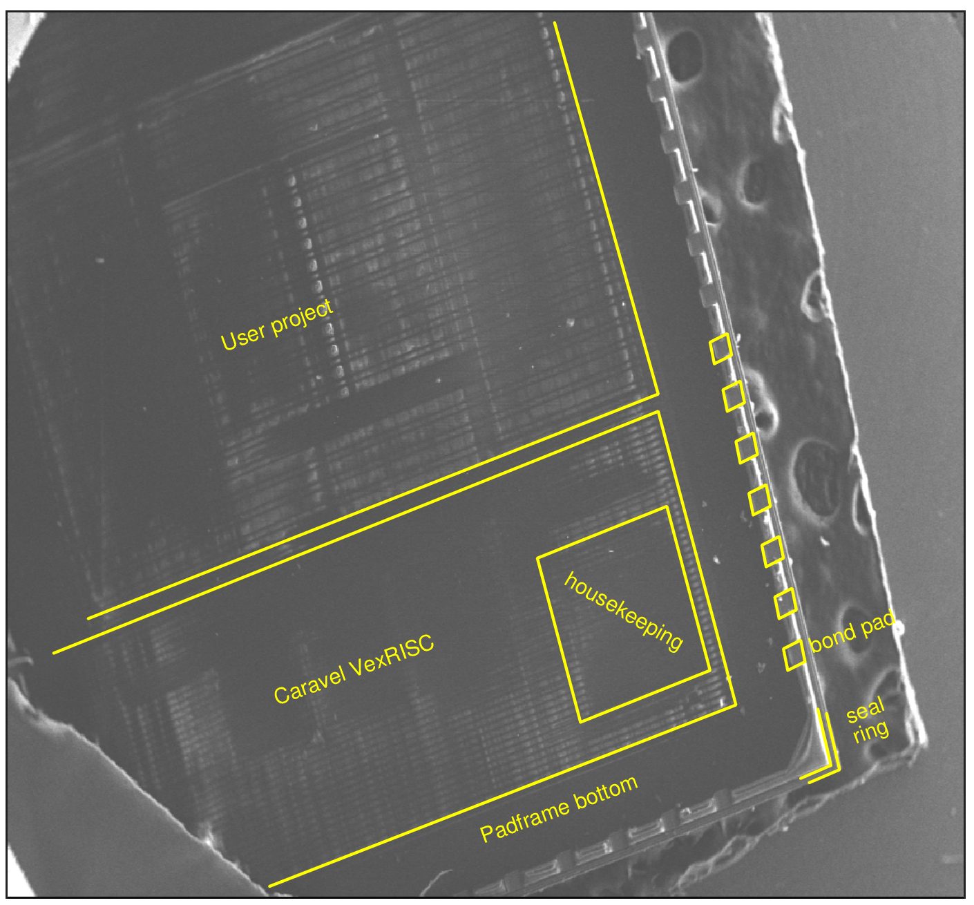
That's definitely Caravel; I can identify the major blocks. Where the layout is visible, it looks like the darker lines are the power distribution network; The horizonal lines would be top level metal, and the vertical lines are the metal under that. Not much else is visible. As to what kind of passivation is on top of the chip, I really don't know. I would not expect anything unusual.
q3k
Hey there! Hope this is the right place to ask, got directed here by Matt. I threw an efabless OpenMPW GF180 die under the SEM today (not sure which shuttle this was, I was gifted this by a friend who wanted to get some SEM shots of it). Did not do any prep to the die other than cleaning, expected to see the topmost metal layer across whatever passivation later might be on top, same as with the SKY130 dies from an earlier OpenMPW run. However, the die was fully opaque to BSE and only very light contours of... CMP pads? Maybe PDN? were visible with SE imaging. Even at 30kV! Is this just that GF180 has one damn thick passivation layer on top, or am I missing something?
First photo is SE, second is BSE.
(The bright thing in the bottom left corner is copper tape for better sample conductivity. I cannot promise that this is standard procedure for sample prep. The bubbly thing to the right is conductive double-sided tape.) (edited)
As we just discussed with Matt - this is likely top polyimide passivation layer, which is likely present on GF180.
q3k
Hey there! Hope this is the right place to ask, got directed here by Matt. I threw an efabless OpenMPW GF180 die under the SEM today (not sure which shuttle this was, I was gifted this by a friend who wanted to get some SEM shots of it). Did not do any prep to the die other than cleaning, expected to see the topmost metal layer across whatever passivation later might be on top, same as with the SKY130 dies from an earlier OpenMPW run. However, the die was fully opaque to BSE and only very light contours of... CMP pads? Maybe PDN? were visible with SE imaging. Even at 30kV! Is this just that GF180 has one damn thick passivation layer on top, or am I missing something?
First photo is SE, second is BSE.
(The bright thing in the bottom left corner is copper tape for better sample conductivity. I cannot promise that this is standard procedure for sample prep. The bubbly thing to the right is conductive double-sided tape.) (edited)