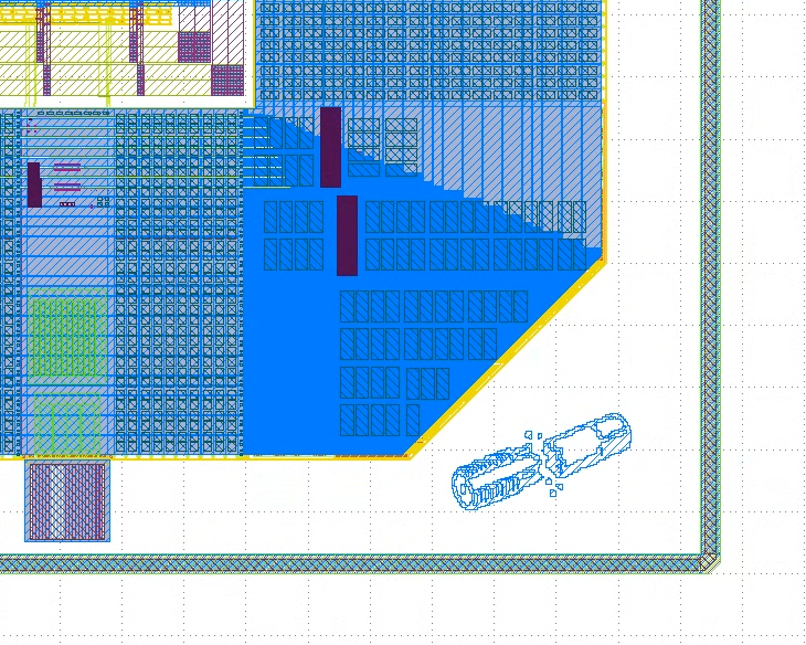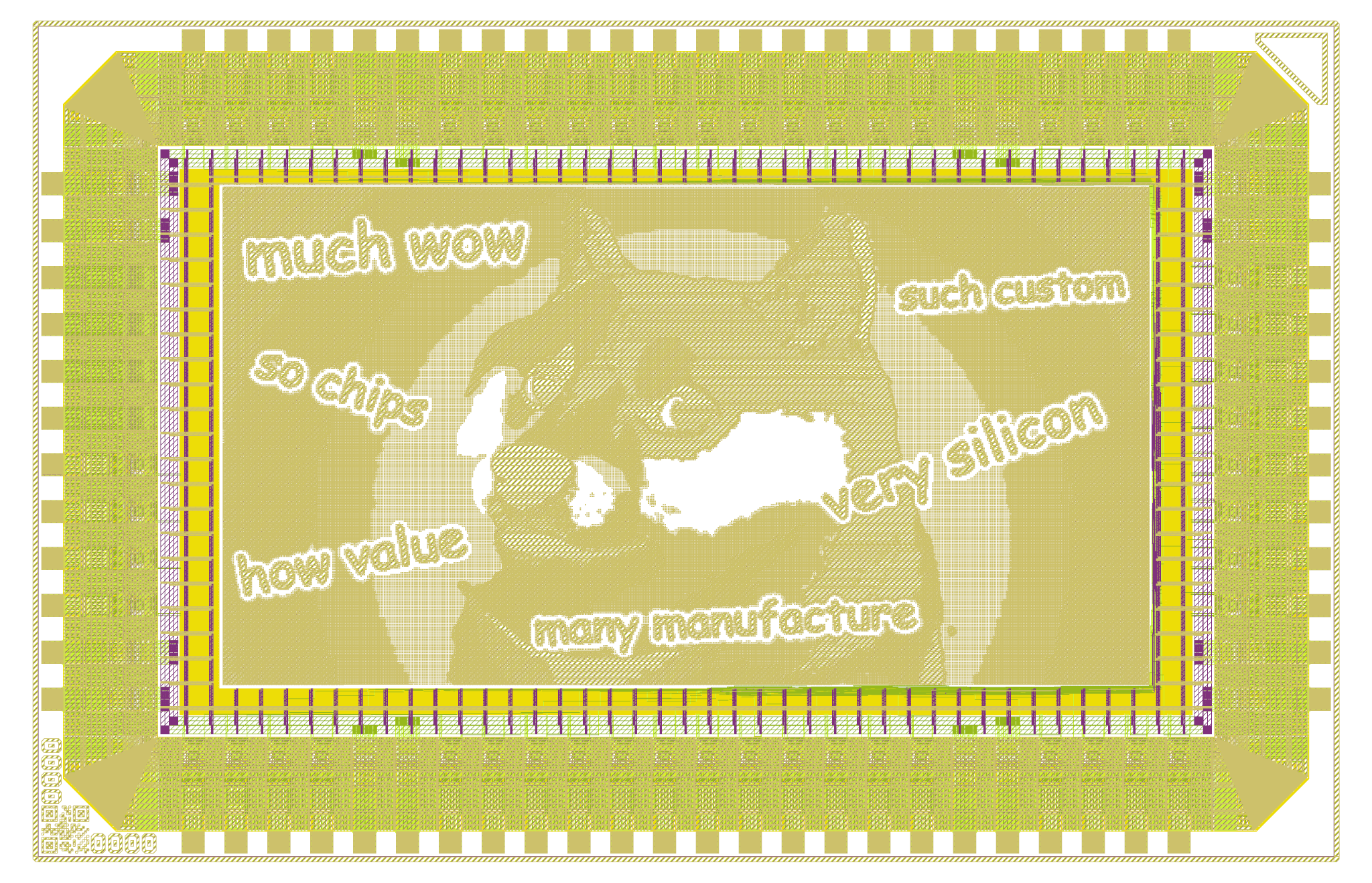
Can i add custom chip art on the top and bottom right corner ( similar to the wafer space logo and qr in the left ) ? Or can i only add inside the pad ring ?
Deepak
Can i add custom chip art on the top and bottom right corner ( similar to the wafer space logo and qr in the left ) ? Or can i only add inside the pad ring ?
yep, you can! I have a little image on the bottom right of mine. I think the top right may be reserved for an arrow this time around (to help the wirebonding alignment) so I think we can't use that corner
BreakingTaps
yep, you can! I have a little image on the bottom right of mine. I think the top right may be reserved for an arrow this time around (to help the wirebonding alignment) so I think we can't use that corner
You are also free to replace the wafer.space logo on the top left. The precheck only checks the bottom left and the top right, if you have CoB enabled.
@BreakingTaps It was mentionned at FSiC last year but ... Not really open. If you look at it there is not much there. You get a standard cell library but only abstract view, no GDS. No DRC rules or any device simulation model. So you can "assemble" a chip with purely digital design but nothing more, nothing custom, ...
1
5:02 a.m.
So you can do basically the same you can do with a FPGA.
Next week at FSiC 2026, we'll be introducing the latest updates on the ics55 pdk, eda tools, and design platform, etc. We have also upgraded the ics55 pdk from tier1 to tier 0. Moving forward, we're planning the roadmap, restructuring the repo based on sky130, gfmcu180, ihp130, and will be gradually releasing the remaining files over the next some months.
Andrew Wingate
I'll just leave this here....
-# Sometimes I feel I should not be allowed to use tools
Maybe we should indeed re-evaluate your permission to use tools
2
Machine Kid myyerrol
Next week at FSiC 2026, we'll be introducing the latest updates on the ics55 pdk, eda tools, and design platform, etc. We have also upgraded the ics55 pdk from tier1 to tier 0. Moving forward, we're planning the roadmap, restructuring the repo based on sky130, gfmcu180, ihp130, and will be gradually releasing the remaining files over the next some months.
Yes, we have integrated the ics55 pdk to ECOS Studio, but now it can only generate partial gds because of some key files haven't be released, so we need to do some works (like DRC/LVS/PEX) by ourselves.
4:58 a.m.
I read the IHP's slide at the FSiC 2026, their pdk and open mpw shuttle is fantastic, so we will learn from ihp sg13g2, to port more open-source eda tools to ics55, and release remaining data as soon as possilbe.
5:04 a.m.
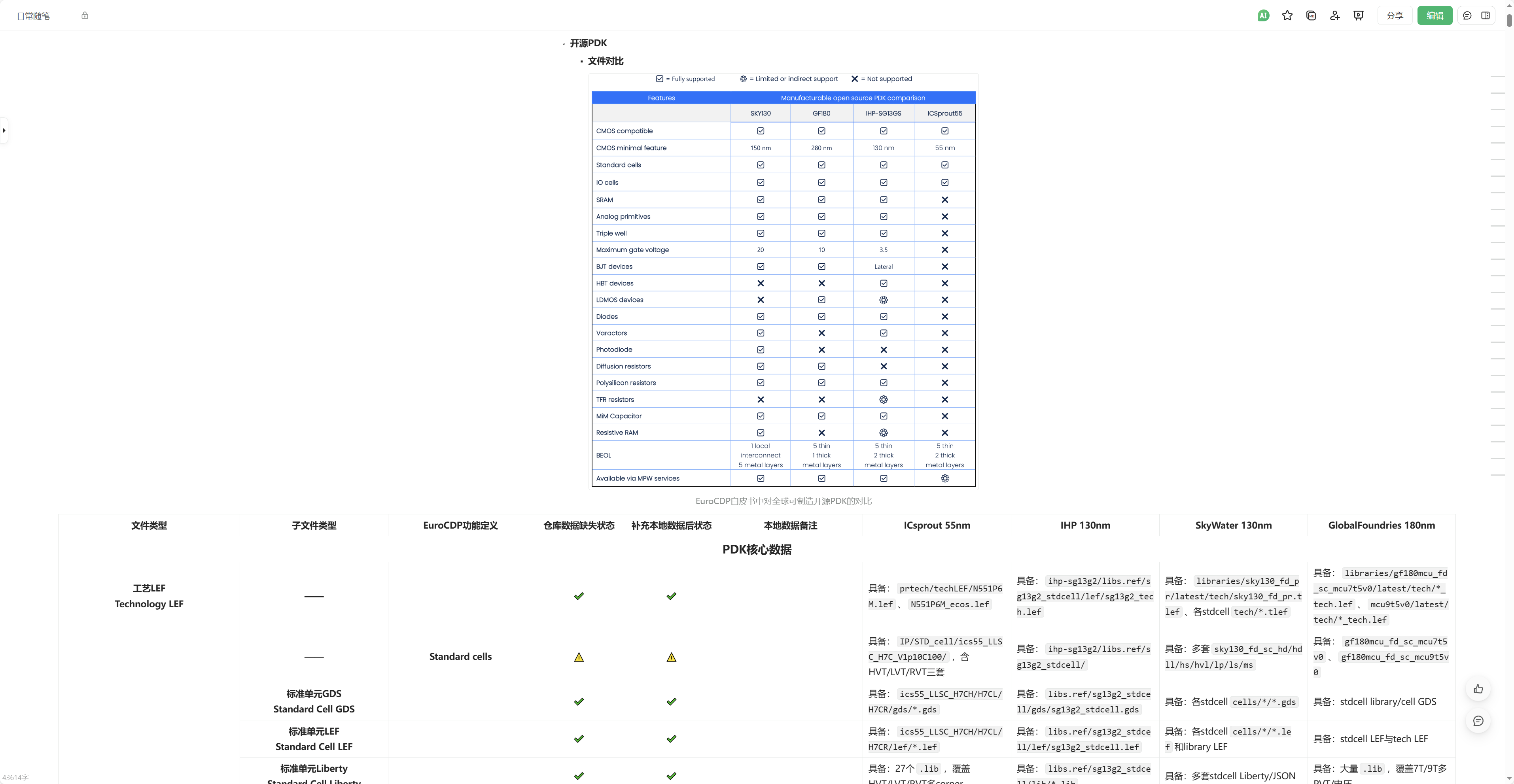
And "EuroCDP Open-source PDKS and EDA tooling recommendations" book also give us great help-a good comparison table.