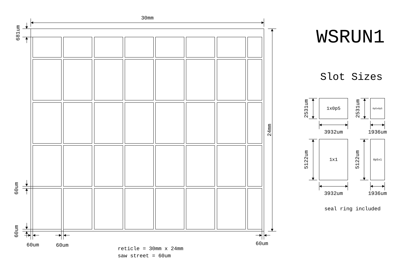
Hey all, I will be meeting with the place that's dicing the wafers. Again this time, they're requesting we back-grind the wafers. We're looking to reduce costs as best we can.
I have a list of questions here. Can anyone think of any better (more) questions to ask?
-----
What saw street widths would allow us to dice without backgrinding?
What width for multi pass cut?
What width for single pass cut?
If we are able to provide 250um would that be sufficient?
What types of saws exist and what type of trade offs between them?
What information is most useful when planning dicing schemes
Is single reticle detail, and general reticle in wafer sufficient?
Would another filetype be better? DXF, etc?
What is the primary driver of cost? Dicing time? Config set up? Saw type?
How is pricing structured: per wafer, per cut, per program setup, per die picked?
If we are able to provide 250um would that be sufficient?
250um seems quite wide to me and would probably mean that we need to remove a few slots from the reticle.
Perhaps we should just ask what width would be strictly necessary, instead of leading with a number.
60um
-# I can't seem to locate the run2 sheet easily, but it's the same.
1
Leo Moser (mole99)
If we are able to provide 250um would that be sufficient?
250um seems quite wide to me and would probably mean that we need to remove a few slots from the reticle.
Perhaps we should just ask what width would be strictly necessary, instead of leading with a number.
Agreed, I think my frame of questioning basically sounds like...
Thicker wheels can more aggressively cut -- BUT these larger wheels chip more. (some of my experience as a machinist)
This also means consumables costs go down, machine cost goes down
But the cost in silicon goes up (larger saw street)
I'm sure we'll go around and around and they won't give me an answer, I've done this before, but in the end I think they'll guide us towards our optimal solution.
Just writing down a thing I heard.
It was referencing backside chipping.. How much do we even care about that? as long as it doesn't affect the front, we are good??
Not sure how much of an issue it is, but AFAIU the chipping is mostly a source/starting point for fracture under mechanical stress, so given the form factor where we pretty much push on the chip to put it in maybe that's something to watch for.
Alright, I guess I'll continue the discussion here.
Today I went to Disco and talked with their engineers, they were great people and gave a lot of great information.
Just writing down a thing I heard.
It was referencing backside chipping.. How much do we even care about that? as long as it doesn't affect the front, we are good??
When I was meeting with Poh I asked first, "do you know anyone at Kulicke & Soffa" as they are headquartered near my hotel and they make the (best, most, one of those words) wirebonders and he said no.
I then asked "do you know any wirebonders?"
And he said "Yeah! Literally downstairs, you want me to call him?"
I obviously said yes lol.
The guy didn't really have a lot of useful information that was sharable. He sent me to this product and while it does have specs it wasn't what I was hoping for.
The one dimension I kept asking about was the length based on die height. The spec we used said 1.5x height, @stuart said 2x, but this guy was very adamant those were wrong and you can go super close, it depends on the capillary you get. He drew some stuff on the whiteboard for me and then erased it before I could take a pic. He then pointed me at this company SPT There's a bunch of stuff to read there, but haven't clicked a link, but they sell the capillaries.
This is the product page for the UTC-RZ1 new generation high-speed wire bonder.Yamaha Robotics is a turn key provider in the field of semiconductor back-end processing and electronic component mounting.
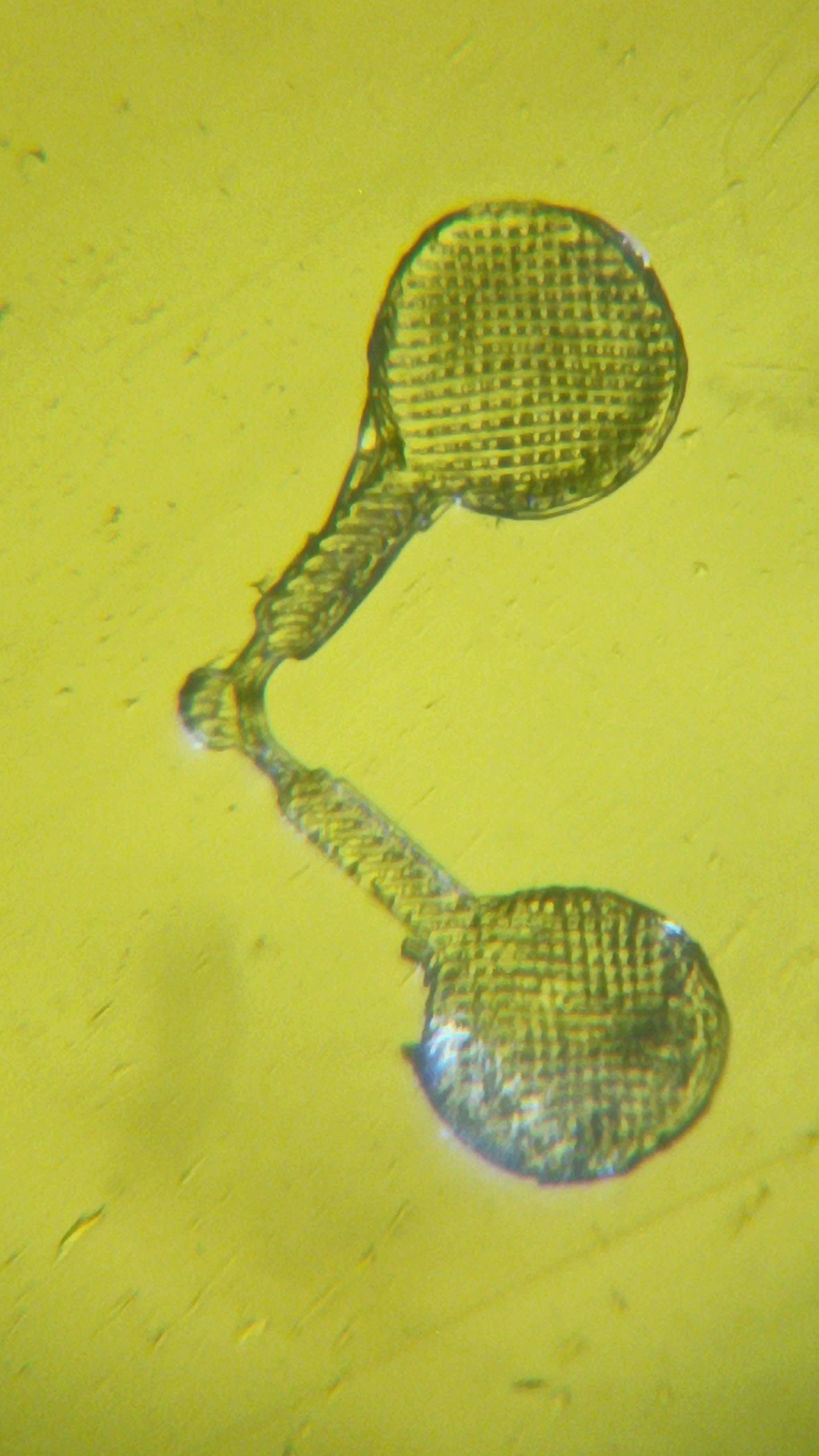
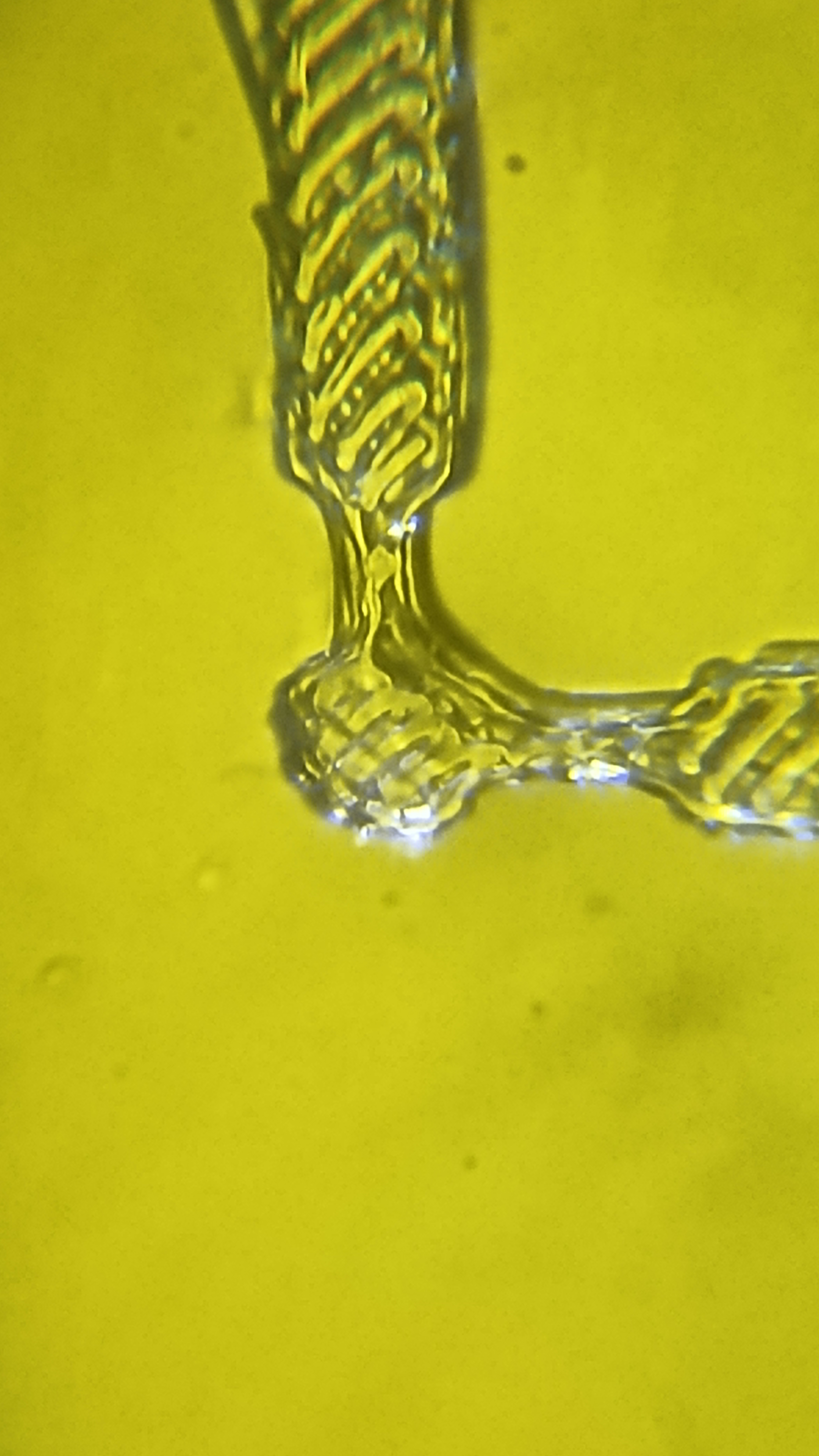
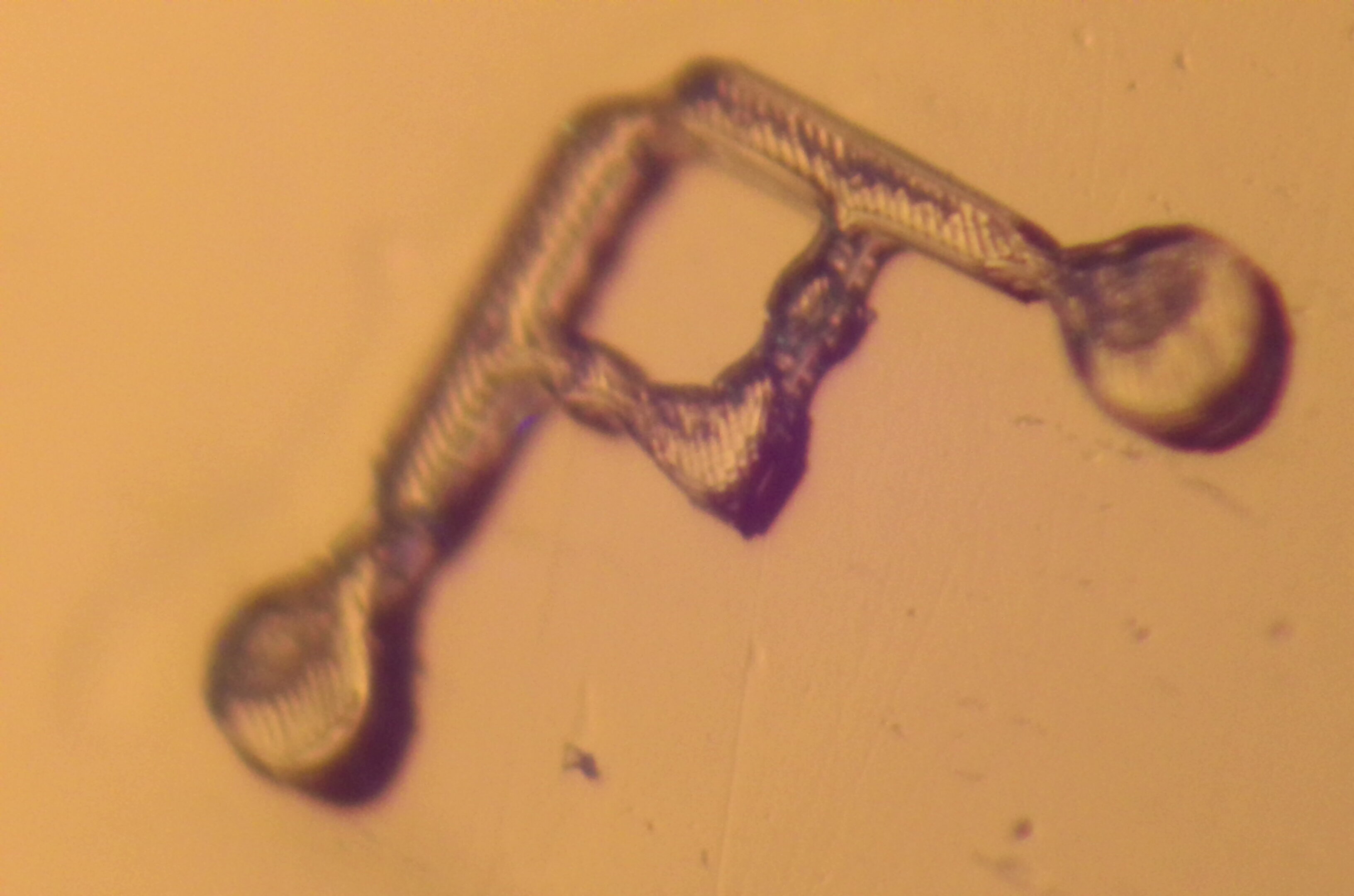
Okay, got the printing working on μRepRap (RepRapMicron). Oh, and put the files/code on github. Here's a test double flexure joint on test pads, done with a path width of 10μm (buy me a damned coffee after this marathon, I'm shaking like a ba*'d! https://ko-fi.com/viksworkshop). It moves. Video to prove it https://youtu.be/ayUqUoDeVxs(edited)
https://www.youtube.com/watch?v=-mgqq0qdDRM I think I'll see to build one of these soon, to at least allow manual pick-and-place for some flip chip testing, given that no opportunity that doesn't essentially rely on my doing it myself has so far come up.
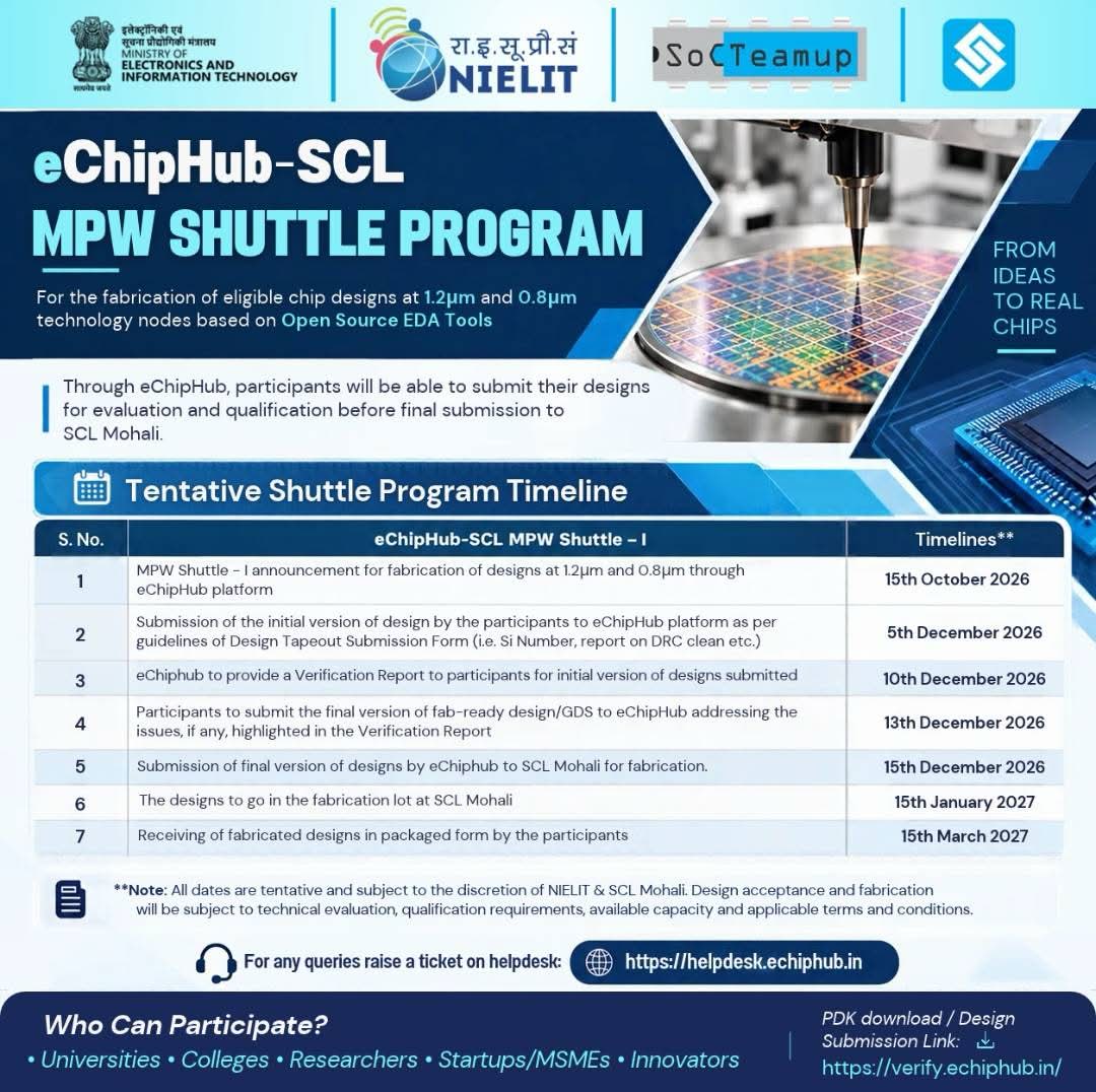
The scl in INDIA has opened two of its old nodes and they are also running mpw for it
Just wanted to know what do tou guys think of this
Please don’t consider it as marketing.
The scl in INDIA has opened two of its old nodes and they are also running mpw for it
Just wanted to know what do tou guys think of this
Please don’t consider it as marketing.