Guild icon
wafer.space Community
𐦂𖨆𐀪𖠋 - Friends / charz
Channel for the discussion around development of better characterization of open source process technologies such as GF180MCU. This includes development around;
  • Physical layout of test structure designs
  • Simulation and TCAD of test structures
  • Collection of real world results from test structures
  • Understanding the PCM (process control monitoring) structures that already exist
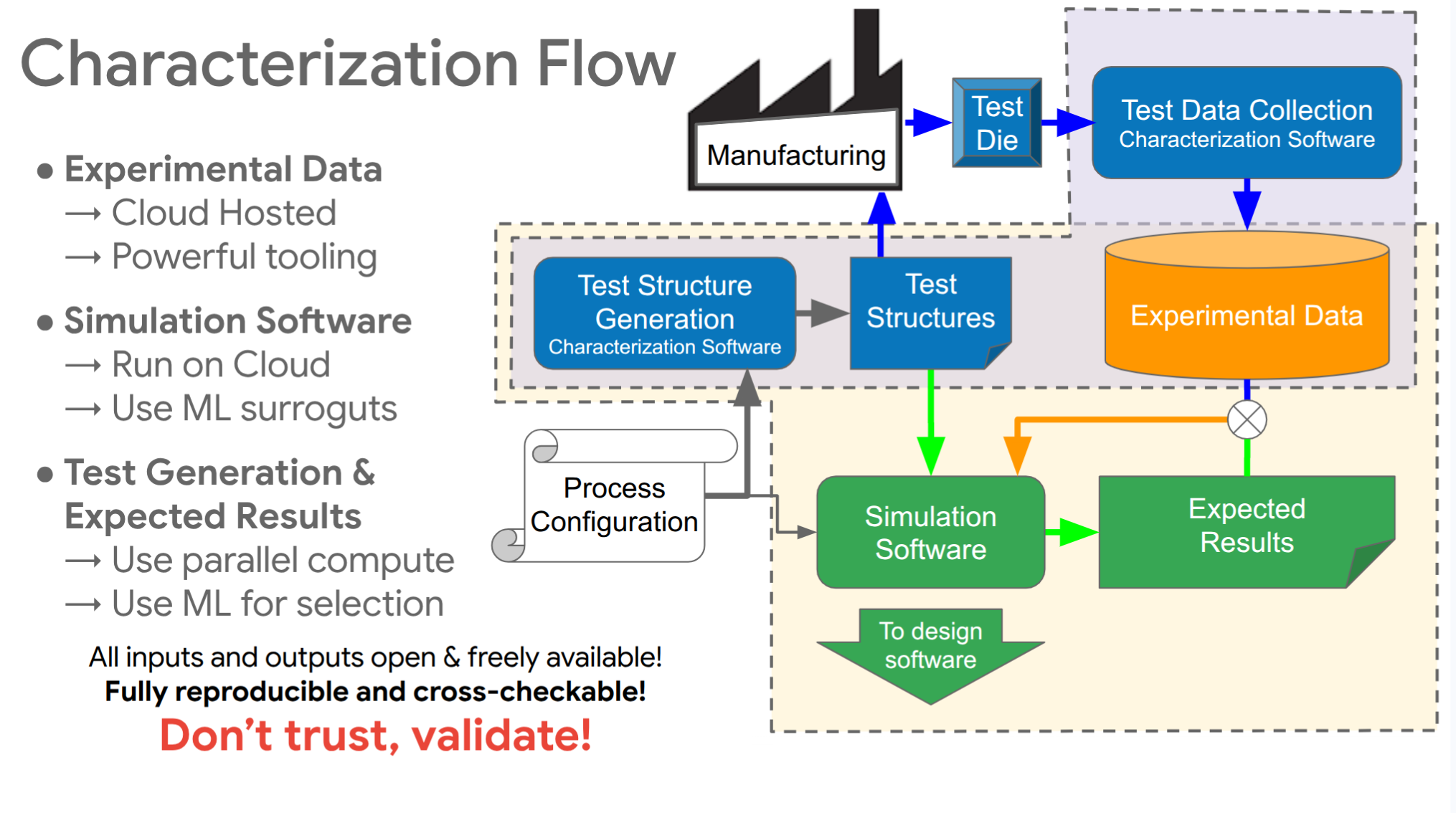
Example details can be found @ https://bit.ly/test-open-pdk
Between 2026-09-30 11:59 p.m. and 2026-11-01 12:00 a.m.

Avatar
Tim 'mithro' Ansell 2026-10-19 2:13 a.m.
@Tim 'mithro' Ansell 's high level thoughts can be found at https://bit.ly/test-open-pdk
Test structure generation and measurement For improving open source PDKs bit.ly/test-open-pdk Owner: Tim ‘mithro’ Ansell <me@mith.ro> Contributors: XXX Last Updated: 2023 Q1 Goal The goal of this document is to provide a central point for the (automated) development of test structures and...
Tim 'mithro' Ansell pinned a message to this channel. 2026-10-19 2:13 a.m.
Avatar
Tim 'mithro' Ansell 2026-10-19 2:14 a.m.
@namibj / @Andrew Wingate / @lromor / @baragonaru / @digshadow - Channel created!
2:14 a.m.
@Leo Moser (mole99) - Who was the person at CERN who did the TRID chip on Run #1?
2:17 a.m.
Other random / shower thoughts from me.
  • I believe we have a bunch of designs on Run #1 and Run #2 that could already be used for some type of initial characterization.
(edited)
2:18 a.m.
Avatar
Tim 'mithro' Ansell 2026-10-19 2:20 a.m.
@Joaquin Matres - I think there was a bunch of people from the GDS Factory team that were also interested in this topic.
2:22 a.m.
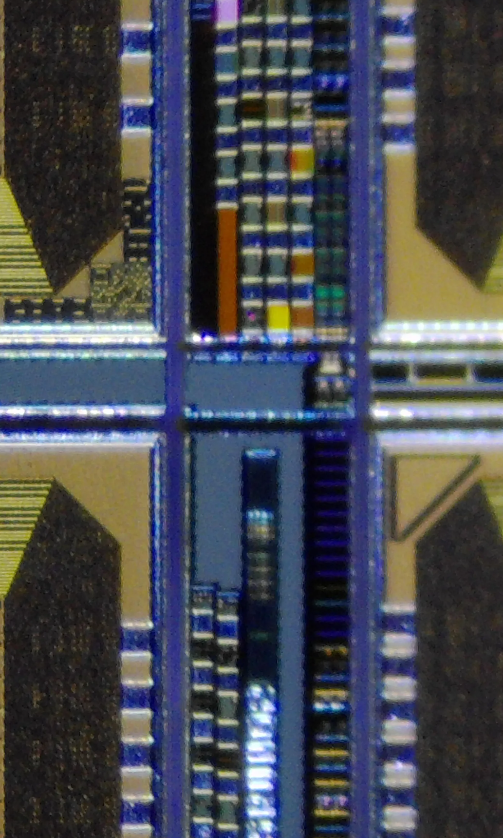
We also has thousands (like >20k) "tiny slivers" of the PCM structures that GF uses to test their wafers are being manufactured correctly. These slivers are left over after we pick people's project die. We don't actually know what the various pads do but we do get etest data from GF which means we do kind of know "what" functionality they might offer. It is also unclear if the pads are actually accessible as they might be used only during manufacturing and then get polyimide over the top of them. @Andrew Wingate can post some pictures of them here.
Avatar
Andrew Wingate 2026-10-19 2:23 a.m.
2:23 a.m.
Not sure run3 is an option unless it's run through @Paul as the reticle is (over)full as it is.
Avatar
Avatar
Tim 'mithro' Ansell
We also has thousands (like >20k) "tiny slivers" of the PCM structures that GF uses to test their wafers are being manufactured correctly. These slivers are left over after we pick people's project die. We don't actually know what the various pads do but we do get etest data from GF which means we do kind of know "what" functionality they might offer. It is also unclear if the pads are actually accessible as they might be used only during manufacturing and then get polyimide over the top of them. @Andrew Wingate can post some pictures of them here.
Andrew Wingate 2026-10-19 2:24 a.m.
2:24 a.m.
2:24 a.m.
Avatar
I want to propose to port/convert the gf180mcuD 3.3V and 5/6V FETs to PSP 103 (though that seems to be kinda EOL recently, and evolved/major-version-switched to PSP 104 that's just a bit incompatible but would be more capable and I think could be used to code the (iirc heavily in geometry restricted by the DRCs we're subjected to, thus making it much easier to bend the PSP model card to represent that LDMOS structure, even if it's not made to be used for modeling flexibile-geometry LDMOS structures) 10V LDNMOS and 10V LDPMOS we get). It's numerically far nicer than BSIM4, which should help with nonlinear convergence especially if arc length continuation is used or for things like harmonic balance: ...and adjoint-sensitivity-based "efficient" monte-carlo/bayesian-style polynomial chaos expansion:
  • basically if you compute through backpropagation the sensitivity to meaningful output measurement numbers as a function of all the monte carlo affected input random variables,
  • you can use that with knowledge of the input variation distributions (which you sample from for monte carlo anyways),
  • to pick far more efficient samples than random monte carlo
  • for the goal of providing a good stochastic estimate of some measure of the distribution of those output measurement numbers: example is expected chip yield for a target +-5% cutoff.
Also the numerical cleanliness should aid in numerically model-fitting based on statistically significant DUT samples, through clean and thus optimizer-friendly backpropagation gradients.
Avatar
Avatar
Tim 'mithro' Ansell
We also has thousands (like >20k) "tiny slivers" of the PCM structures that GF uses to test their wafers are being manufactured correctly. These slivers are left over after we pick people's project die. We don't actually know what the various pads do but we do get etest data from GF which means we do kind of know "what" functionality they might offer. It is also unclear if the pads are actually accessible as they might be used only during manufacturing and then get polyimide over the top of them. @Andrew Wingate can post some pictures of them here.
Do you have masks for those regions? It'd be great to at least do some looking to maybe figure out what's going on there. Is that e-test data in some form that's "interpretable" without needing to look at some NDA'd docs? Like, from a file format POV?
2:41 a.m.
I don't think polyimide top coating over the PCM structures should prevent probing. A sharp probe should have no issues penetrating that soft material. If there's oxide that'd be less harmless
Avatar
Tim 'mithro' Ansell 2026-10-19 2:41 a.m.
What is PSP?
2:41 a.m.
@namibj - BTW Have you seen the previous work by SemiMod?
Avatar
Looking at this suggests the PCM pads to be the same surface as the COB-targeted bond pads on the wafer.
Avatar
Avatar
Tim 'mithro' Ansell
@namibj - BTW Have you seen the previous work by SemiMod?
not particularly
2:46 a.m.
For reference, the IHP SG13 core transistors in openPDK are coded in PSP 103.
Avatar
and given that IHP SG13 is an RF-focused process family with it mostly existing/being created for supporting their Si:Ge HBT application research efforts, I'd tend to trust their usefulness for analog and RF circuits more than the legacy BSIM stuff that's source-referenced (meaning the math gets unfortunately fairly gnarly inside if you accidentally extract a source as a drain because their model doesn't feel like computing in a way that numerically doesn't care if source is source and drain is drain (or they are swapped)) and also this should allow more effective coding of bent gates as a result from the math being cleaner. Also offers self-heating, as an aside. And might not need (nearly as) aggressive binning to work well.
Avatar
Avatar
Tim 'mithro' Ansell
@Leo Moser (mole99) - Who was the person at CERN who did the TRID chip on Run #1?
Leo Moser (mole99) 2026-10-19 1:28 p.m.
That's Clyde! @Clyde Laforge
Avatar
Avatar
Leo Moser (mole99)
That's Clyde! @Clyde Laforge
Indeed! I have not done characterisation yet, as I still need to receive the pcb, but these should come very soon
Avatar
Count us in. We sign off at SS 85 °C / 3.135 V, and our SS85 Liberty is derived from the shipped SS125. An audit this week found that boils down to a single ~0.959 scale on every delay table, so we'd really like silicon data to see how far off that is. We can help with Liberty/STA analysis, proposing timing DUTs (per-cell ring oscillators, SRAM access paths), the digital side of the muxed e-test harness, and measured data from our own Run 3/4 dies. (edited)
Avatar
Avatar
Andrew Wingate
Not sure run3 is an option unless it's run through @Paul as the reticle is (over)full as it is.
we still have some allocation left!
Avatar
Avatar
Paul
we still have some allocation left!
Andrew Wingate 2026-10-19 7:45 p.m.
Awesome! Not sure if you've met @namibj Sorry, @namibj I haven't had the time to give your proposal the time it deserves. Would/ do you have the time/interest in completing some of these for Run3? Want to pin down some reasonable goals/expectations if so? Thanks and sorry, I don't have the capacity to contribute, but am happy to facilitate wherever possible. -# side note: @Paul I have sent out some feelers to other folks, I think they were interested in Serdes, I should hear back from them tonight.
Avatar
you’re being really helpful. would you want to get on a call with me after you hear back from the folks? just want to learn more about what Serdes is
Avatar
Avatar
Paul
you’re being really helpful. would you want to get on a call with me after you hear back from the folks? just want to learn more about what Serdes is
Andrew Wingate 2026-10-19 7:47 p.m.
Sure thing!
❤️ 1
Avatar
Tim 'mithro' Ansell 2026-10-20 1:00 a.m.
@Paul - Have you seen https://bit.ly/open-pipe-talk -- that is not really connected to this #charz channel though?
SERDES, PIPE and protocols Pathway to fully open source implementations... Presenters Tim ‘mithro’ Ansell <tansell@google.com> bit.ly/open-pipe-talk
1:01 a.m.
@Agenxy - BTW Who are you?
Avatar
Tim 'mithro' Ansell 2026-10-20 5:15 a.m.
I'm still behind in reading everything on discord - but this might be useful -> https://gist.github.com/mithro/596e9249d1aa26f1482620f33e33ecc1
wafer.space GF180MCU: run 1 and run 2 projects useful for process characterisation - gf180mcu-characterisation-projects.md
Avatar
Avatar
Tim 'mithro' Ansell
@Paul - Have you seen https://bit.ly/open-pipe-talk -- that is not really connected to this #charz channel though?
excellent! totally get it now
💜 1
Avatar
Avatar
Tim 'mithro' Ansell
@Agenxy - BTW Who are you?
Hey Tim, sorry, just saw this! Agenxy is my small independent open-silicon lab in SF; I'm an SoC debug/perf engineer by background. I'm building an open RV64 Linux SoC aimed at wafer.space Run 4, plus a small RISC-V MCU. We sign off at SS85 derived from your shipped SS125 libs, hence the interest in #charz. Your Run 1/2 characterisation gist is really useful, thanks.
Avatar
Tim 'mithro' Ansell 2026-10-21 12:14 a.m.
I have no idea what SS125 and SS85 mean 😛
12:15 a.m.
Open-silicon lab means things like SoC design?
12:15 a.m.
@Agenxy -^
Avatar
Avatar
Andrew Wingate
Awesome! Not sure if you've met @namibj Sorry, @namibj I haven't had the time to give your proposal the time it deserves. Would/ do you have the time/interest in completing some of these for Run3? Want to pin down some reasonable goals/expectations if so? Thanks and sorry, I don't have the capacity to contribute, but am happy to facilitate wherever possible. -# side note: @Paul I have sent out some feelers to other folks, I think they were interested in Serdes, I should hear back from them tonight.
the muxed e-test proposal?
Avatar
Avatar
Tim 'mithro' Ansell
I have no idea what SS125 and SS85 mean 😛
slow-slow corner at that temperature.
3:27 a.m.
I can almost certainly mentor what's needed on the actual coding/scripting front of it. As I've been a bit broken these past couple months I'm unlikely to manage to get enough in the flow on enough of the days left to do the coding myself, though, sadly.
Avatar
Avatar
Agenxy
Count us in. We sign off at SS 85 °C / 3.135 V, and our SS85 Liberty is derived from the shipped SS125. An audit this week found that boils down to a single ~0.959 scale on every delay table, so we'd really like silicon data to see how far off that is. We can help with Liberty/STA analysis, proposing timing DUTs (per-cell ring oscillators, SRAM access paths), the digital side of the muxed e-test harness, and measured data from our own Run 3/4 dies. (edited)
I'd love to hear if a muxed e-test chip that can give 4-wire-style measurements (two mux lines routed to each DUT LEF pin) at effectively DC conditions would be expected to allow sufficient calibration of the models with the SPICE around based on fine-tuning/fitting the extracted models to really fit the e-test results, as we could expect to measure such e-test over an entire batch of a thousand dies. I think a full die should work for about 300 DUTs if they're fairly large, or if they're SCL mix without being heavy on many-pin combinatorials probably up to around 500 DUTs. The spacing along the mux array for the "width" of a DUT's slot is given by M4 min pitch and how many wires that needs. All but GND I was planning on having two wires (GND only a sense, as drive/force is part of the latch up prevention globally distributed substrate taps). I was planning on harnessing Sandia National Laboratories 's Dakota and Xyce tools to do uncertainty quantification to accompolish an approximation to optimal experiment design to pick a set of "interesting" sample points, which would be voltages and/or currents applied at each of the drive pins. I also want to get data on vias and contacts (the PDK gives extremely wide and quite high magnitude resistance values for them) as well as thin oxide native NMOS and what's needed for local missmatch modeling of those devices where that isn't yet covered by the PDK's SPICE models.
Avatar
Tim 'mithro' Ansell 2026-10-21 10:27 a.m.
Contribute to EngGhaith/RLCM-Test-Passives-For-GF180MCUD development by creating an account on GitHub.
10:28 a.m.
Contribute to EngGhaith/RLCM-Test-Passives-For-GF180MCUD development by creating an account on GitHub.
Avatar
Avatar
Tim 'mithro' Ansell
I have no idea what SS125 and SS85 mean 😛
haha fair, SS125 is the slow-slow process corner at 125°C, it's the timing lib wafer.space ships, I sign off at 85°C so I derive my own from it. and yeah open-silicon lab as in chip/SoC design with open PDKs and open tools, and we release the designs openly
Avatar
Avatar
namibj
I'd love to hear if a muxed e-test chip that can give 4-wire-style measurements (two mux lines routed to each DUT LEF pin) at effectively DC conditions would be expected to allow sufficient calibration of the models with the SPICE around based on fine-tuning/fitting the extracted models to really fit the e-test results, as we could expect to measure such e-test over an entire batch of a thousand dies. I think a full die should work for about 300 DUTs if they're fairly large, or if they're SCL mix without being heavy on many-pin combinatorials probably up to around 500 DUTs. The spacing along the mux array for the "width" of a DUT's slot is given by M4 min pitch and how many wires that needs. All but GND I was planning on having two wires (GND only a sense, as drive/force is part of the latch up prevention globally distributed substrate taps). I was planning on harnessing Sandia National Laboratories 's Dakota and Xyce tools to do uncertainty quantification to accompolish an approximation to optimal experiment design to pick a set of "interesting" sample points, which would be voltages and/or currents applied at each of the drive pins. I also want to get data on vias and contacts (the PDK gives extremely wide and quite high magnitude resistance values for them) as well as thin oxide native NMOS and what's needed for local missmatch modeling of those devices where that isn't yet covered by the PDK's SPICE models.
I'd expect DC 4-wire to get the device params pretty well (Vt, Idsat, the via/contact resistances you mentioned), and a good SPICE fit re-characterised at 85°C would already be better than my flat scale. the thing DC won't see is capacitance though, and that's a big part of delay, so would it make sense to add a few ring oscillators per key cell/drive strength with an on-die divider so the same low speed tester can read frequency? that would check delay directly, and measuring at 2 temps would check the derating too. happy to share my corner data and review the structure list
Avatar
Andrew Wingate 2026-10-22 8:21 p.m.
8:21 p.m.
@Tholin I would like to test multiple versions. Would it be ok/better/whatever to have one of your cpu select to save pins, or how many pins can I use? -# forwarding here as it's a little more on topic
Avatar
You can use all of the digital IOs
8:34 p.m.
But then you’d need to power up the digital section of the chip
Avatar
Avatar
Tholin
But then you’d need to power up the digital section of the chip
Andrew Wingate 2026-10-22 8:37 p.m.
I feel like I'm hitchhiking so am trying to have as small a footprint as possible. Sounds good. I should have something for you hopefully tomorrow?
8:38 p.m.
*also thank you!!
Avatar
You have a lot of area
8:40 p.m.
A whole quarter of the die is unused
Avatar
Avatar
Andrew Wingate
I feel like I'm hitchhiking so am trying to have as small a footprint as possible. Sounds good. I should have something for you hopefully tomorrow?
looks like we might not have a full muxed e-test die this tapeout, but whatever we do, if your sensor would have worked inside a tinytapeout with some extra parasitic capacitance on the bus/shared pad's wires (on the far side of "your" analog mux switch), focusing on DC-characterizing some missing devices with not so many pins instead of really covering some high-pin-count SCL combinatorics, like perhaps having local mismatch modeling for shottkey diodes and have modeling at all for thin oxide native threshold nmos), might be worthwhile to try and combine those efforts at least for this Run3?
Avatar
given that analog would need custom probe pads I don't think it'll work well on that there.... sadly.
👍 1
thankyou 1
Avatar
See here how much free space there is on my die:
1:12 p.m.
Avatar
Avatar
namibj
Click to see original message
@Agenxy opinion?
Exported 62 message(s)
Timezone: UTC+0