I'm currently designing the PCB for my chip on wsrun #1, but I can't quite wrap my head around the pinout of the mezzanine connectors.
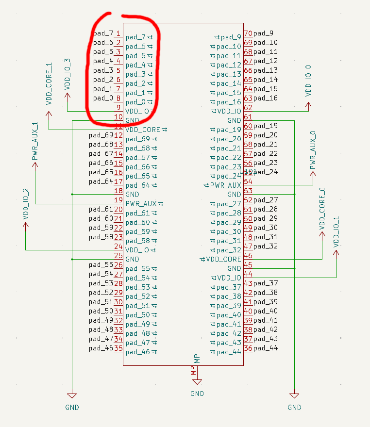
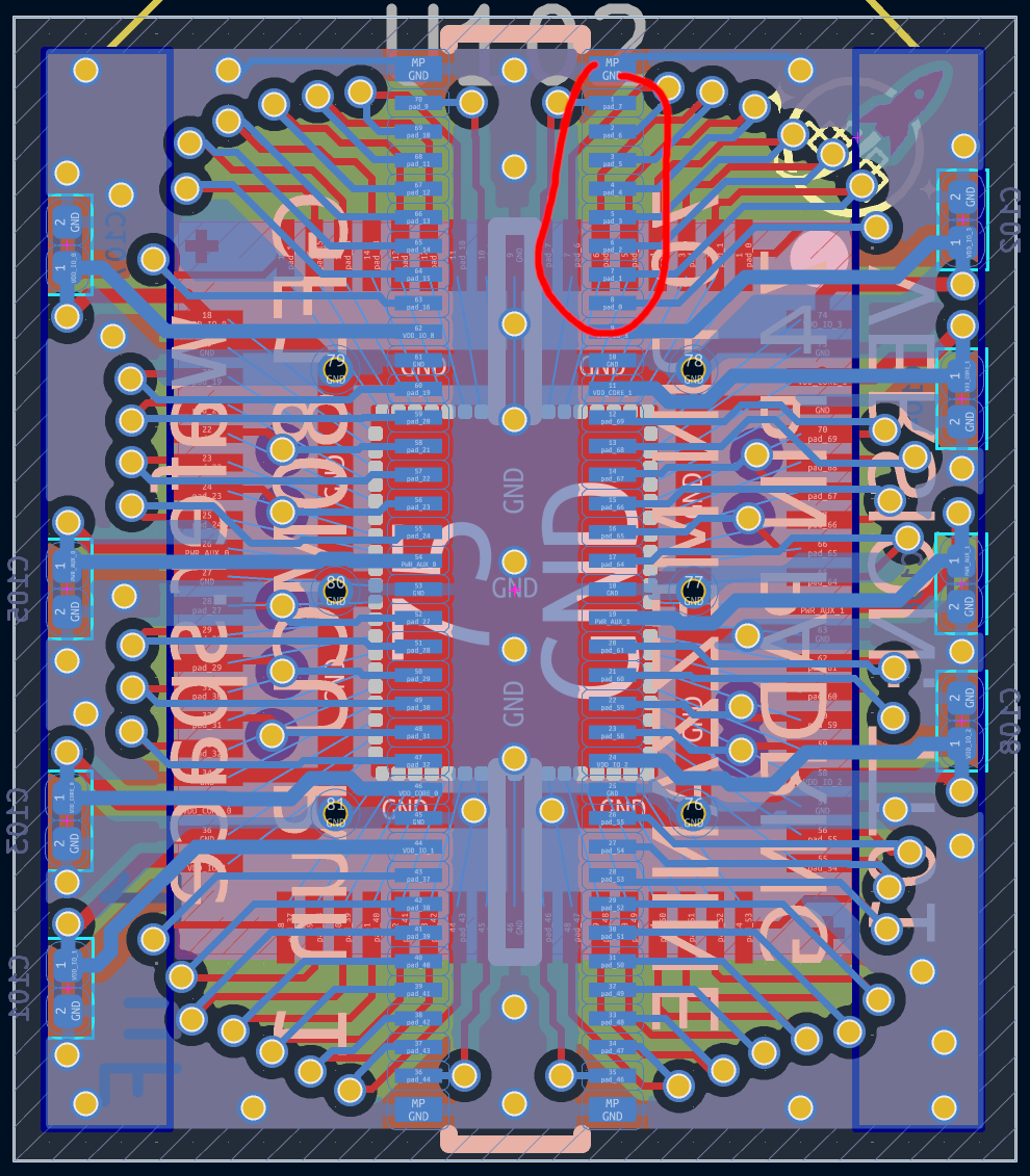
This is from the 1x1-cob:
7:18 a.m.
7:18 a.m.
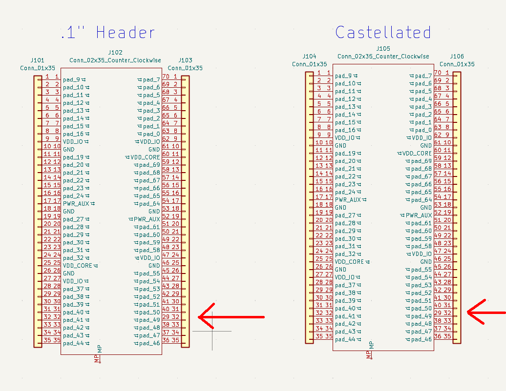
The connector is on the backside, and viewing the backside from above (through the PCB), pad7 to pad0 are in the top right corner.
Now, when I take this CoB PCB and plug it into a female mezzanine connector on the motherboard, I would still expect pad7 to pad0 to be in the top right corner, since the mezzanine connector doesn't swap sides, right?
7:18 a.m.
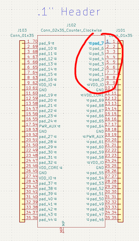
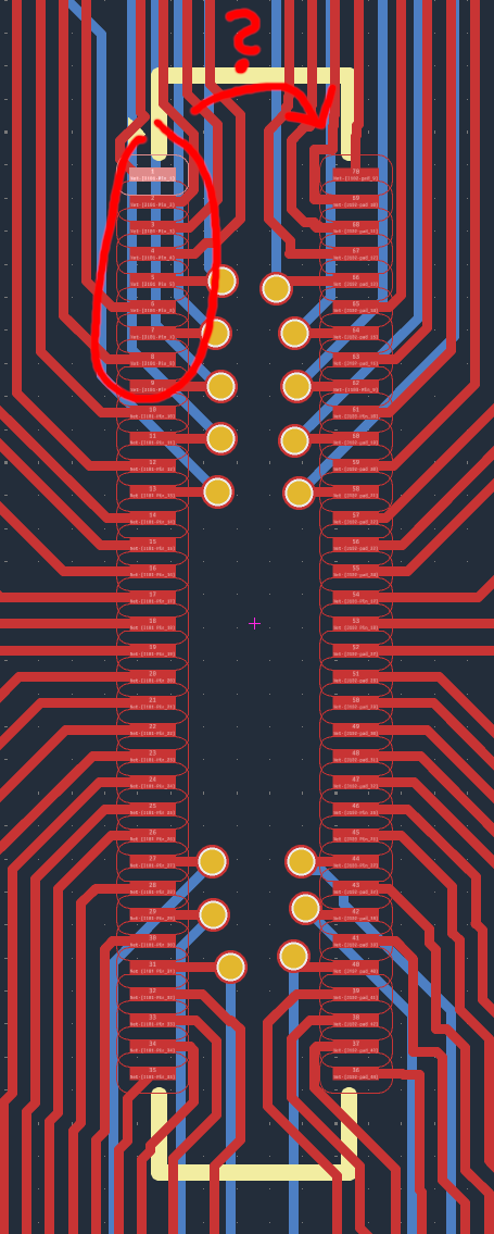
Taking a look at the motherboards in the same folder, I can see that pad7 to pad0 are suddenly in the top left corner on the motherboard.
7:19 a.m.
7:19 a.m.
Why is that the case? If the mezzanine connector simply connects down, they should be in the top right corner?
Does anyone see the same thing, or am I missing some important point :)
Browser viewable link: https://kicanvas.org/?repo=https%3A%2F%2Fgithub.com%2Fwafer-space%2Fchip-on-board-wire-bonded-pcbs%2Ftree%2Fmain%2Frun-1%2F1x1-cob
The mezzanine is on the back side. So the first schematic is backwards if you're looking through the cob only correct if you're looking from the back
When you plug it into the motherboard you're looking through the cob making the second schematic the correct version of what to look at
-# the copper (and more to the point labels) on the second post are incorrect! I need to make a new symbol that has pin1 in the correct location with respect to the mezzanine connector and not the cob itself.
Again sorry for the confusion.
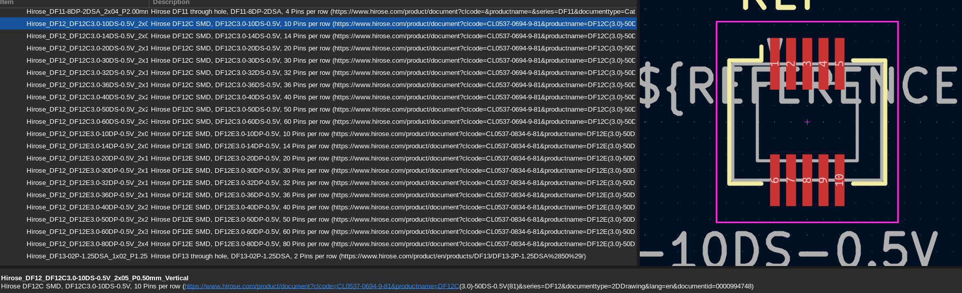
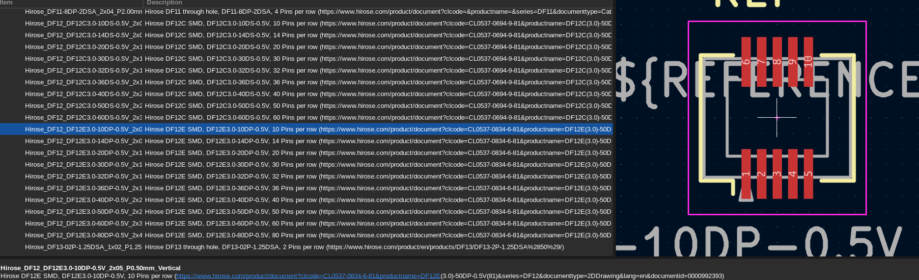
Kicad has other examples of DP / DS connectors footprints like Hirose DF12.
DP should have pin 1 on the lower left and DS should have pin 1 on the upper left.(edited)
Sure, I'm not saying you did, I'm just saying if we fix them to actually be coherent with each other, of the two options, we should pick the one that matches what kicad standard lib does (edited)
I am likely going to flip it for run2? IDK we'll see how people feel about it.
We're likely going to be rethinking from first principles run3+ and the padring pinouts will likely be changing to better suit the different sizes more harmoniously.
I think this is the same thing that BreakingTaps and I ran into. The motherboards have their pins flipped. I made a fixed version of the breadboard breakout here: https://codeberg.org/rebelmike/ws-breakout
I also have a fixed version of the footprint with a box outlining where the CoB covers and the wafer space logo in the correct corner of that box in use here: https://codeberg.org/rebelmike/ws01-tinyQV-mobo-alpha(edited)
(Although obviously I haven't actually tested these yet as I have no CoBs)
RebelMike
I think this is the same thing that BreakingTaps and I ran into. The motherboards have their pins flipped. I made a fixed version of the breadboard breakout here: https://codeberg.org/rebelmike/ws-breakout
I also have a fixed version of the footprint with a box outlining where the CoB covers and the wafer space logo in the correct corner of that box in use here: https://codeberg.org/rebelmike/ws01-tinyQV-mobo-alpha(edited)
Thank you, Mike! This confirms what I was seeing (and I thought I was going crazy ><). The left and right sides of pins are flipped on the motherboard.
I'll use your breakout as reference for designing my PCB.
6:30 p.m.
@Andrew Wingate This means that if someone uses the run-1/motherboards and relies on the pad names, their PCB won't work since the pins are flipped.




 (edited)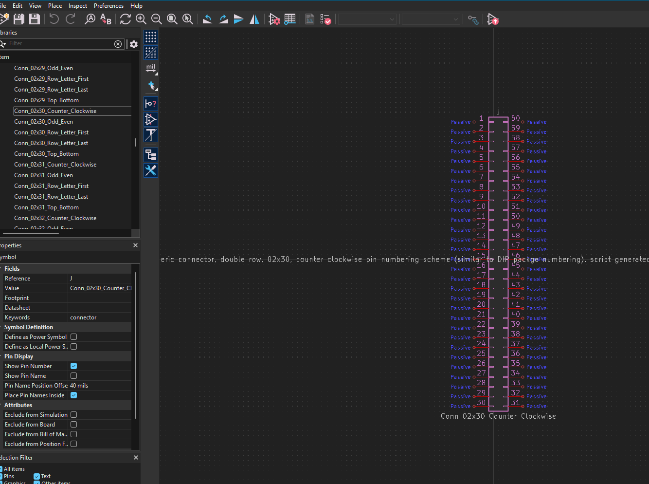

 1
1