
wafer.space Community
🏗️ - Designing / project-template / Magic errors
Between 2025-10-31 11:59 p.m. and 2025-12-01 12:00 a.m.

Error while reading cell "chip_top" (byte position 97630252): Warning: cell "Metal4_fill_cell" placed on top of itself.  Ignoring the extra one.
Error while reading cell "chip_top" (byte position 97630316): Warning: cell "Metal1_fill_cell" placed on top of itself.  Ignoring the extra one.
Error while reading cell "chip_top" (byte position 97630380): Warning: cell "Metal4_fill_cell" placed on top of itself.  Ignoring the extra one.
Error while reading cell "chip_top" (byte position 97630628): Warning: cell "Metal1_fill_cell" placed on top of itself.  Ignoring the extra one.
Error while reading cell "chip_top" (byte position 97630876): Warning: cell "Metal3_fill_cell" placed on top of itself.  Ignoring the extra one.
Error while reading cell "chip_top" (byte position 97630980): Warning: cell "Metal4_fill_cell" placed on top of itself.  Ignoring the extra one.
However, having checked the layout, I don't think I have any cells placed on top of themselves. Could it be because KLayout creates arrays for the filler cells?...
1570000 uses
1575000 uses
1580000 uses
[21:39:22] ERROR Error while reading cell "chip_top" (byte position 120711644): cell power_route_01_a_512x8m81 was used but not defined.
[21:39:22] ERROR Error while reading cell "chip_top" (byte position 120711644): cell M1_PSUB4310591302014_512x8m81 was used but not defined.
[21:39:22] ERROR Error while reading cell "chip_top" (byte position 120711644): cell G_ring_512x8m81 was used but not defined.
......
Cell power_route_01_a_512x8m81 read from path /home/leo/Repositories/gf180mcu-project-template/gf180mcu/gf180mcuD/libs.ref/gf180mcu_fd_ip_sram/mag
...Processing timestamp mismatches.
Timestamp mismatches found in these cells: M1_NACTIVE_02_512x8m81, M1_NWELL_01_512x8m81, M1_PACTIVE$10_512x8m81, M1_PACTIVE$11_512x8m81, M1_POLY2$$204150828_512x8m81, M1_POLY24310591302019_512x8m81,
M1_POLY24310591302031_512x8m81, M2_M1$$204138540_512x8m81, M2_M1$$204139564_512x8m81, M2_M1$$204140588_512x8m81, M2_M1$$204141612_512x8m81, M2_M1$$204220460_512x8m81, M2_M1$$204221484_512x8m81,
M2_M1$$204222508_512x8m81, M3_M2$$204142636_512x8m81, M3_M2$$204143660_512x8m81, M3_M2$$204144684_512x8m81, M3_M2$$204145708_512x8m81, M3_M2$$204146732_512x8m81, M3_M2$$204147756_512x8m81,
nmos_1p2_01_R270_512x8m81, nmos_1p2_02_R90_512x8m81, nmos_5p04310591302099_512x8m81, nmos_5p043105913020111_512x8m81, pmos_1p2_01_R90_512x8m81, pmos_1p2_02_R90_512x8m81, pmos_5p043105913020101_512x8m81,
...
Could I have made a mistake when updating the PDK from open_pdks? I'm not even sure if I touched the SRAM at all.# Read in maglef views in order to blackbox cells
if { [info exists ::env(MAGIC_DRC_MAGLEFS)] } {
foreach {maglef} $::env(MAGIC_DRC_MAGLEFS) {
puts "Loading maglef view: $maglef"
load $maglef
}
}
But I'm also reading the GDS afterwards. Does the GDS perhaps overwrite the mag view?
 1
1gds noduplicates truegds noduplicates true # Enable gds noduplicates to ignore cells
# that have been previously loaded as maglef
gds noduplicates true
gds readonly true
# Flatten cells
if { [info exists ::env(MAGIC_GDS_FLATGLOB)] } {
foreach {gds_flatglob} $::env(MAGIC_GDS_FLATGLOB) {
gds flatglob $gds_flatglob
}
}used but not defined errors will occur if the source file doesn't define cells in bottom-up order. You might need to use gds ordering true before reading in. However, I'm not sure that there is any obvious consequence beyond the error message as long as the cell is defined later in the file.used but not defined errors will occur if the source file doesn't define cells in bottom-up order. You might need to use gds ordering true before reading in. However, I'm not sure that there is any obvious consequence beyond the error message as long as the cell is defined later in the file. gds noduplicates true after reading in the mag, right?noduplicates after reading in the maglef layouts. Probably best for me to just look at the layout myself with the abstract SRAM view and see what it looks like and what DRC errors are getting reported. I assume that will be in the same chip_top layout?lef write -hide). That will be a huge LEF file, but it will be accurate with respect to the metal layers. I'm not sure it will properly represent diffusion and poly. The better solution is (2) do not create fill patterns inside the area of the SRAMs.explode the cell instance array through scripting, but neither method managed to separate the filler cells.
At least it's not a blocking issue.
2. The maglef covering up the layers makes a lot of sense! Thanks for the hint.
I would rather not prevent fill inside the SRAMs since this PDK only allows to restrict filler generation on all metal layers.
I removed the -hide argument from open_pdks. The resulting maglefs are 10MB in total (not ideal), but now the fill is correctly inserted.
3. Yes, I already flatten comp and poly2 fill cells. That's not an issue on my side:
  MAGIC_GDS_FLATGLOB:
  # COMP and Poly2 filler cells need to be
  # flattened to form a "filltrans" layer
  - "COMP_fill_cell"
  - "Poly2_fill_cell"
MAGIC_DRC_MAGLEFS in LibreLane was that I hadn't loaded the maglef views. I had loaded the mag views  ♂️
By loading the maglef views, all the DRC errors are resolved. Well, actually, not all of them. By using the maglefs from the current PDK I still got some Metal3 spacing errors in the SRAM periphery. Using the no
♂️
By loading the maglef views, all the DRC errors are resolved. Well, actually, not all of them. By using the maglefs from the current PDK I still got some Metal3 spacing errors in the SRAM periphery. Using the no -hide maglefs resolved all of the DRC errors within the SRAM macro.
Could you run magic DRC on the PDK maglefs on your end to confirm my suspicion?
Still, the question is whether we really want to distribute 10MB maglefs for the SRAMs just to avoid checking the DRC rules inside it?
Even if we don't implement the 5V/3.3V SRAM rules, it probably makes more sense to use the SramCore layer to skip these DRC checks in the area.
This way I don't need to update the wafer.space precheck every time a new SRAM is generated, and users could generate their own SRAMs.
Even if we don't implement the 5V/3.3V SRAM rules in magic, in the worst case violations should get caught by KLayout.
How difficult would it be to disable specific rules in a certain layer through the magic tech file? 1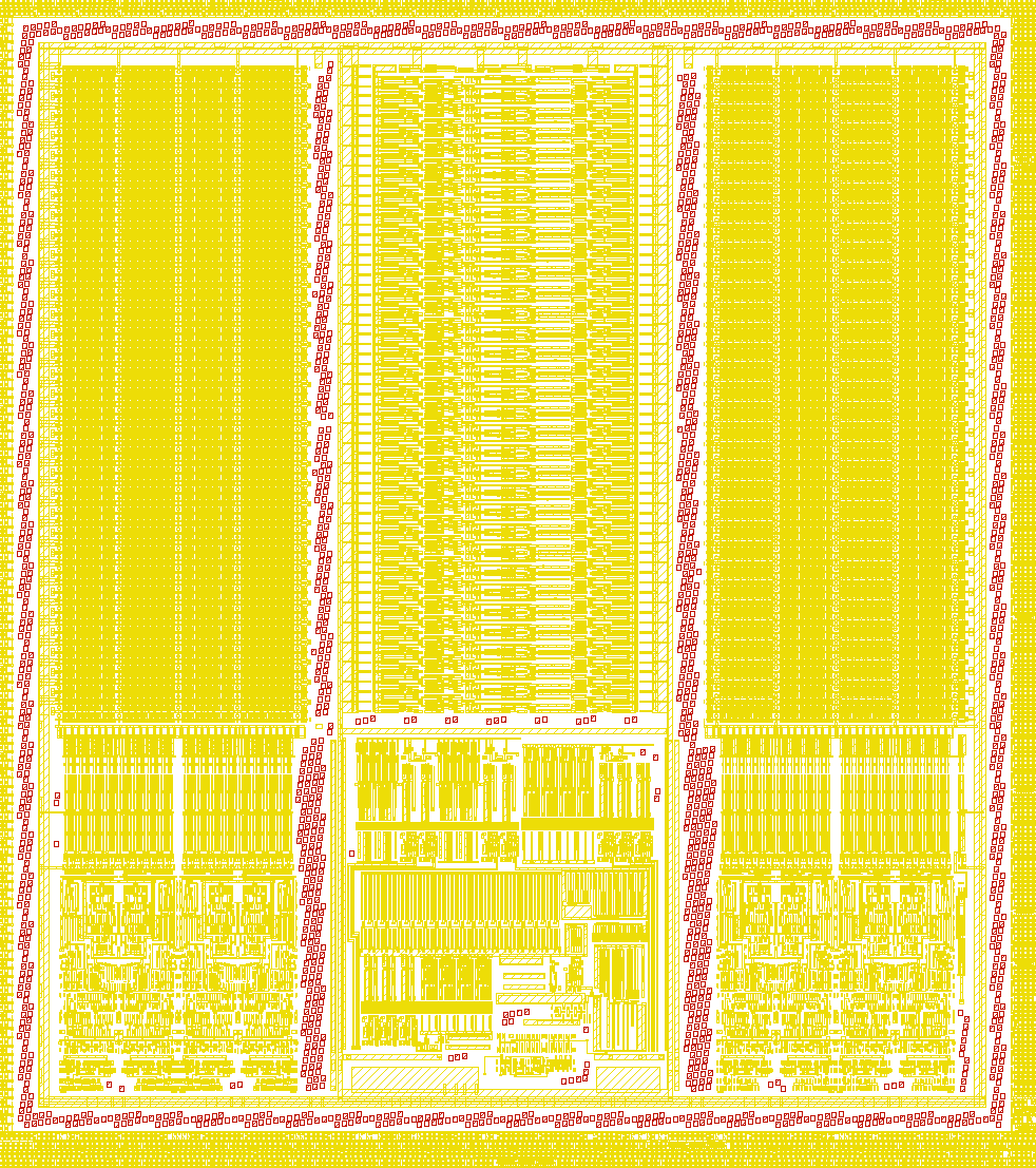
SramCore layer.
This is essentially what we already do with the maglef view, but it works on all SRAMs with the SramCore layer without the need to read in the maglef. PORT
LAYER Metal3 ;
RECT 118.435 30.885 206.985 30.995 ;
END
So it might be worthwhile just to find all the errors (which I don't think are that many---There is only the one error in the 64x8 SRAM) and eliminate those port entries from the upstream repository LEF views. For now, the maglef without the
 -hide option works well, and 10MB more isn't the end of the world (ciel can even deduplicate the PDK variants).
Ideally, magic could also run directly on the GDS of the SRAM. Initially, by ignoring the 5V/3.3V SRAM rules, and later maybe even by implementing them.
How would the first part be implemented, i.e. how would certain rules be ignored in the SramCore layer?SramCore.
PL.5a is implemented as follows:
 spacing allpolynonfet alldifflvnonfet 100 corner_ok allfets \
    "Poly spacing to diffusion < %d (PL.5a)"
 spacing allpolynonfet alldiffmvnonfet 300 corner_ok allfets \
    "Poly spacing to MV diffusion < %d (PL.5a)
Can I just remove all poly that is inside SramCore from allpolynonfet? How would I do that? I absolutely agree, the DRC shouldn't be based on cells. That's why the PDK provides the
 SramCore layer (108/5). The foundry SRAMs use this layer to mark the SRAM bit cells.
Yes, I would rather not generate a detailed abstract view. But this is the only way we can generate the fill afterwards. It would be possible to clean up the detailed views slightly by replacing the the bitcell array with an obstruction.
Ideally, magic could use the GDS directly. I assume people want to create their own SRAM macros for educational purposes, or, in the case of Staf's generator, to generate new SRAM configurations. 1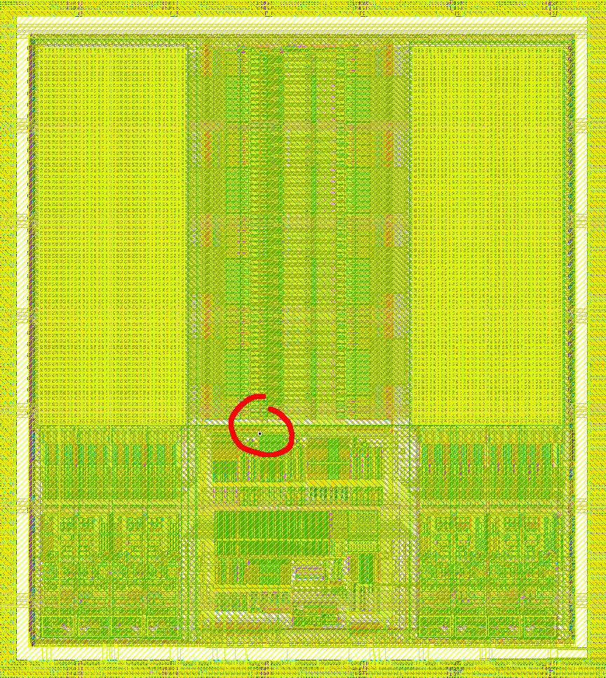
 My PC has 64GB of memory too, but I haven't noticed it filling up yet.