Guild icon
wafer.space Community
📐 - Designing / 📦-cob / 70 pin Mezzanine COB
Between 2025-09-30 11:59 p.m. and 2025-11-01 12:00 a.m.
2:09 p.m.
Pure poetry.
💜 1
Avatar
Beautiful, very versatile 👍 👍
6:04 p.m.
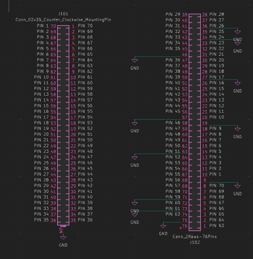
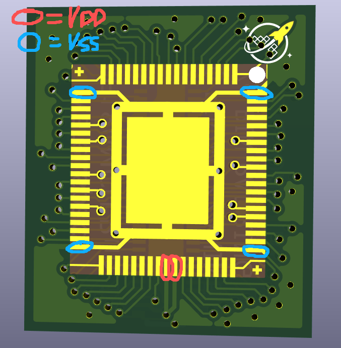
What is the pin assignment? 74 bondpads ==> 74 bondfingers (on PCB), 10 of which are connected to the GND ring, so 64 signal pins including one VDD; do we need that many GND/VSS? How about one on each side, or even one, or even none; the designer can decide how many VSS they want, the inductance of going down to the ring vs to the bondfinger is not going to be that significantly different. Getting access to 74 pins that we can assign ourselves will take this to the next level. If I counted correctly there are 74pins on the connector. (edited)
6:05 p.m.
@Andrew Wingate See above; not sure if this shows in the regular COB channel.
Avatar
There are 70 pins on the connectors, the 4 "outside" ones are not electrically connected or something, datasheet of the connector says to ignore them.
Avatar
Got it, so how about we shoot for 70pins: GND + 69 signal pins that the designers can place, including VDD. So that means we need to use 4 VSS pins. We will have to decide if we want to pre assign VSS to certain bondpads, likely we should. I would recommend bondpads in the corners; the regular bondwires to the bondfingers are longer and so less ideal for signals but that's not an issue for VSS since you are going to the VSS/GND ring which is close. Also, if you plan to put decoupling on the mezzanine board, you will have to decide which pin is VDD also and we all have to follow that convention. So @Andrew Wingate, do you think it is possible to have just 4 pins connected to the VSS ring, one in each corner? If we fix the VDD pin, we should put it in the middle of a side that will have the lowest bondwire inductance. If some projects want to do multiple VDDs they could use the neighboring pins and maybe you can add some footprints for zero Ohm resistors so they can be shorted. I am attaching a PDF to clarify what I am talking about. Top figure is changes to PCB; bottom is rough illustration of what the bonding diagram will look like. When drawing this rough bonding diagram I noticed that the angles in the corners get quite acute. We will have to check with the bonding house if they can support that. Ideally we would also rotate the pads (like in the photo on the wafter.space homepage) to be in line with the wires, that will improve bonding yield. Also moving the bondfingers a bit further out will help with improving the angles. Does this design meet the checks of the slides that @Tim 'mithro' Ansell had shared higher up in this channel? What kind of bondwires are you going for? Gold or aluminum? Many thanks for all the work on this. This approach of a mezzanine board with a connector on the back is a winner in my mind. Very flexible!
Avatar
Thank you @peterkinget @tnt is correct, while there are 74 pads on the connector, only 70 are used electrically.
What is the pin assignment? 74 bondpads ==> 74 bondfingers (on PCB)
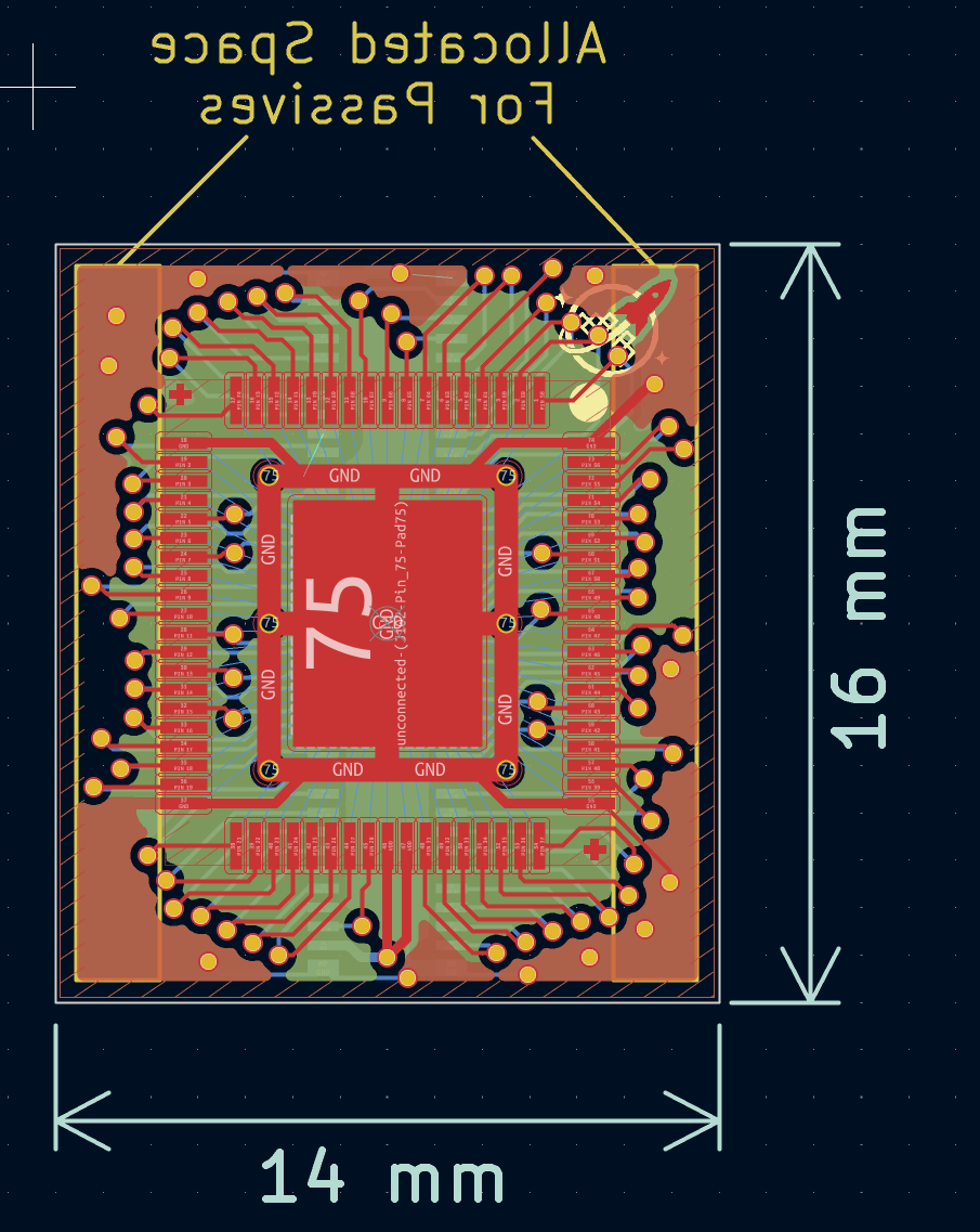
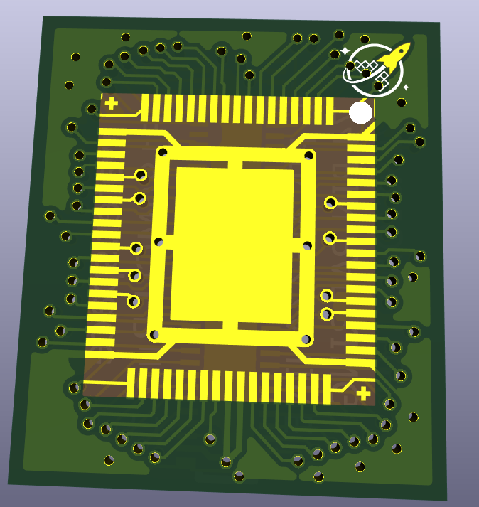
I know that you wouldn’t want to use this COB as is, and I fully expect there will be a number of variations, even if the only difference is the silkscreen version number. For instance, @tnt wants decoupling caps on their COB. This would be very bad for you. But you would may want to add a number of resistors for protection, or have components like leds on the oscillator that never make it to the mezzanine connector or to even create testpads for the extra 4 pins so you still have access. I have identified a zone where we can place any kind of passives--or any component that fits really-- to do with as you like. This is to say, you would have 74 bondpads, but only 70 signals actually make it to the mezzanine connector. Ground/Signal/VSS can be wherever suits you.
What kind of bondwires are you going for? Gold or aluminum?
This is outside my knowledge and @Tim 'mithro' Ansell would have to get back to you on that.
11:55 p.m.
@peterkinget I watched your and @Matt Venn video yesterday. Very cool what you're doing! https://www.youtube.com/watch?v=abu3u6UX6wE
👍 1
Avatar
Avatar
Andrew Wingate
Thank you @peterkinget @tnt is correct, while there are 74 pads on the connector, only 70 are used electrically.
What is the pin assignment? 74 bondpads ==> 74 bondfingers (on PCB)
I know that you wouldn’t want to use this COB as is, and I fully expect there will be a number of variations, even if the only difference is the silkscreen version number. For instance, @tnt wants decoupling caps on their COB. This would be very bad for you. But you would may want to add a number of resistors for protection, or have components like leds on the oscillator that never make it to the mezzanine connector or to even create testpads for the extra 4 pins so you still have access. I have identified a zone where we can place any kind of passives--or any component that fits really-- to do with as you like. This is to say, you would have 74 bondpads, but only 70 signals actually make it to the mezzanine connector. Ground/Signal/VSS can be wherever suits you.
What kind of bondwires are you going for? Gold or aluminum?
This is outside my knowledge and @Tim 'mithro' Ansell would have to get back to you on that.
OK, fair enough, did you share the latest design already. No rush, but let us know when you do and we will update the board a bit.
Avatar
Avatar
Andrew Wingate
@peterkinget I watched your and @Matt Venn video yesterday. Very cool what you're doing! https://www.youtube.com/watch?v=abu3u6UX6wE
Thanks, and many thanks for Matt for hosting me!
Avatar
Avatar
peterkinget
OK, fair enough, did you share the latest design already. No rush, but let us know when you do and we will update the board a bit.
I did not, I am embarrassed.. I will share. Keep in mind that this is likely very fluid, so I'm going to wait to nail things down until we know more.
👍 1
Avatar
Avatar
peterkinget
OK, fair enough, did you share the latest design already. No rush, but let us know when you do and we will update the board a bit.
The pin mapping is the embarrassing part of all this. I should have just made a symbol, but didn't know at the time what to call anything--I think I know now--but probably won't change anything until we know more from wirebonders and such. I have committed the latest designs. https://github.com/wafer-space/chip-on-board-wire-bonded-pcbs
Wire bonded chip on board PCB designs. Contribute to wafer-space/chip-on-board-wire-bonded-pcbs development by creating an account on GitHub.
Avatar
@Andrew Wingate Thank you for your work on this. Just to clear some things up for us, I have couple questions: 1) I saw there are some pins on the COB that are still routed to the ground ring. What what I understand, we can customize each pin to whatever we want (power/signal/ground) and we can choose how many ground pins to have and where to put them, correct? 2) In the case that we switch one of the "original" ground pins to a signal pin, would we delete that metal routing or just the via? 3) Just to be clear, will COB changes be handled by yourself if we hand in a final completed pin list? Or would we perform the changes on our end and confirm it's cost viability with you? (edited)
Avatar
Avatar
asc
@Andrew Wingate Thank you for your work on this. Just to clear some things up for us, I have couple questions: 1) I saw there are some pins on the COB that are still routed to the ground ring. What what I understand, we can customize each pin to whatever we want (power/signal/ground) and we can choose how many ground pins to have and where to put them, correct? 2) In the case that we switch one of the "original" ground pins to a signal pin, would we delete that metal routing or just the via? 3) Just to be clear, will COB changes be handled by yourself if we hand in a final completed pin list? Or would we perform the changes on our end and confirm it's cost viability with you? (edited)
Andrew Wingate 2025-10-19 1:29 a.m.
No problem :) 1) Correct, you can choose whatever pins you want to go wherever you want. Some are easier than others, like I saw @peterkinget had interest in sending VDD out the middle of the top and bottom. While that is fine, it may require moving a lot of pins, or running VDD though some inner layers. All options are fine, but some require more work than others. 2) The traces that go from a bond pad to the ground pin are just traces and can be deleted. All vias can be moved as well. Really anything can be moved. If you want to put some passives in the allocated areas and need to move basically all the traces, that's fine. I think keeping the overall dims to 14x16mm and smt components in the allocated spaces to allow for a generic vacuum chuck, the rest is whatever you can dream up. 3) We'll see how much time I've got around the time this gets nailed down, but I'd be happy to make some changes for you all. We seem to be comfortably in our cost projections at the moment, so anything similar should not change anything. Thanks to you two as well for being so active and creating cool stuff!
❤️ 1
Avatar
I see I see. Thank you for the clarification!
Avatar
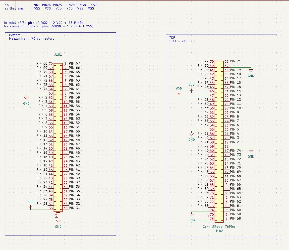
@Andrew Wingate Thank you for your great design of Mezzanine COB, We have made some modifications based on Prof @peterkinget 's suggestions. Right now, there are 2 VDD Pins on Chip (PIN29 and PIN30), 4 VSS Pins on Chip (PIN1, PIN20, PIN38 and PIN57), and 68 Signal Pins.
💜 1
Avatar
We will share on github shortly.
Avatar
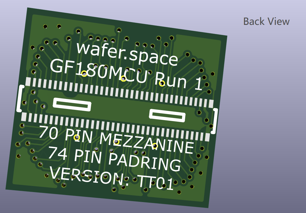
Remove the "Version TT01" silk, this is definitely no longer TT. (edited)
👍 2
Avatar
Thank you for your suggestion
Avatar
PCB design for COB packaging through wafer.space. Contribute to mosbiuschip/WaferSpace_COB_70pins development by creating an account on GitHub.
👍 1
10:40 p.m.
We are now working out a bonding diagram to get a sense of the angles etc. Stay tuned (can be a couple of days).
Avatar
Avatar
xianglin_pu
@Andrew Wingate Thank you for your great design of Mezzanine COB, We have made some modifications based on Prof @peterkinget 's suggestions. Right now, there are 2 VDD Pins on Chip (PIN29 and PIN30), 4 VSS Pins on Chip (PIN1, PIN20, PIN38 and PIN57), and 68 Signal Pins.
Cool, nice work @xianglin_pu. I would definitely run a DRC check. Also thanks @peterkinget. Like I said before, there are likely to be some small changes, but this is a great start. Thank you
👍 2
Avatar
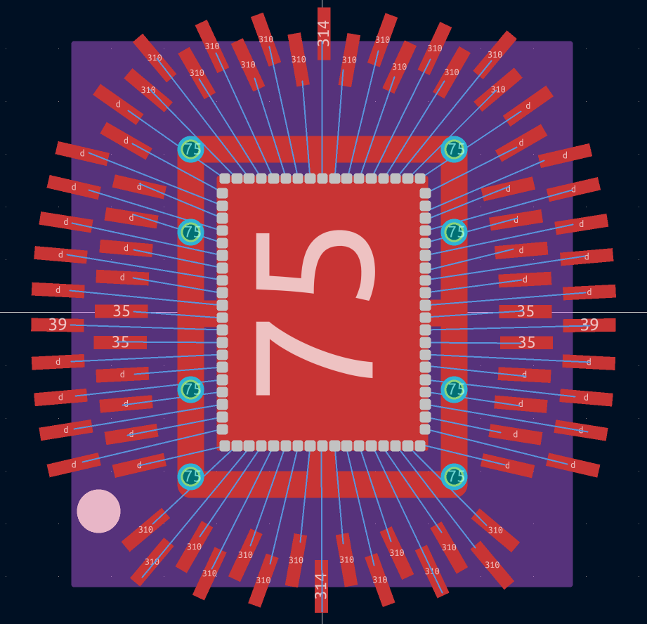
Thanks Prof.@peterkinget's further suggestion in bonding, we have made some modification to the bond pad orientation such that each bond wire can connect to the corresponding bond pad which is perpendicualr to the pad's edge, which benefits in throughput and reliability for connections. (please ignore the numbers on bondpads, they will be updated later based on the design) I have uplodaed the design into github "https://github.com/mosbiuschip/WaferSpace_COB_70pins/tree/xp/mezzanine_round_bond" This is still in progress, and we will keep modifying it and makes it better, any feedbacks are appreciated ! Thank you. (edited)
Avatar
@Andrew Wingate @Tim 'mithro' Ansell @Leo Moser (mole99) what do you think? We are designing the 74 cob so anyone can use it. Only the vss and VDD pads are fixed, all other pads can be freely assigned. We are optimizing the bond finger placement for better bonding yield.
Avatar
Avatar
xianglin_pu
Thanks Prof.@peterkinget's further suggestion in bonding, we have made some modification to the bond pad orientation such that each bond wire can connect to the corresponding bond pad which is perpendicualr to the pad's edge, which benefits in throughput and reliability for connections. (please ignore the numbers on bondpads, they will be updated later based on the design) I have uplodaed the design into github "https://github.com/mosbiuschip/WaferSpace_COB_70pins/tree/xp/mezzanine_round_bond" This is still in progress, and we will keep modifying it and makes it better, any feedbacks are appreciated ! Thank you. (edited)
Andrew Wingate 2025-10-27 8:15 a.m.
Thanks @xianglin_pu and @peterkinget that looks beautiful. A few notes and questions. One of the things we're going for is density on part of keeping the COB PCB itself small as possible. You can see above that I designed the ring, so we could sneak a few vias under the bond wires. I fear this would use up more space in the end. As far as the size of the pads and their spacing, I ended up where we did by attempting to keep the design as loose as possible. Current spacing between pads is .15mm and could easily be .1 while staying in standard 2 layer rulesets. We could even drop down to 0.8mm if we wanted to push it. Same thing for the pads themselves. They're currently .25mm and could easily be cut in half. Following this to it's end actually puts that spacing below what's actually on the die itself. So fundamentally if we wanted we could literally go perpendicular with 0 fanout if we wanted.
Avatar
Avatar
Andrew Wingate
Thanks @xianglin_pu and @peterkinget that looks beautiful. A few notes and questions. One of the things we're going for is density on part of keeping the COB PCB itself small as possible. You can see above that I designed the ring, so we could sneak a few vias under the bond wires. I fear this would use up more space in the end. As far as the size of the pads and their spacing, I ended up where we did by attempting to keep the design as loose as possible. Current spacing between pads is .15mm and could easily be .1 while staying in standard 2 layer rulesets. We could even drop down to 0.8mm if we wanted to push it. Same thing for the pads themselves. They're currently .25mm and could easily be cut in half. Following this to it's end actually puts that spacing below what's actually on the die itself. So fundamentally if we wanted we could literally go perpendicular with 0 fanout if we wanted.
Thank you for your notes, I will carefully check the spaceing between bondpads, right now the minimum space between two pads. I believe from original COB design is around 0.15mm, in the new design case is around 0.2mm as I set clearance area to 0.1mm, and I used same pad size as original one, so should also be .25mm. We will keep optimizing it for VSS down-bonds and via locations etc,.. (edited)
Exported 27 message(s)
Timezone: UTC+0