
wafer.space Community
📐 - Designing / 🕰️-analog / The current KLayout deck reports an
Between 2026-05-31 11:59 p.m. and 2026-07-01 12:00 a.m.

poss_4_4_via1 = via1.sized(0.2, 'square_limit').merged.sized(-0.2, 'square_limit').and(metal1).and(metal2)
The magic tech file already has 2 spacing rules for vias, but it's based on the size of the via region.
 templayer via1large via1
        shrink 915
        grow 915

 layer VIA1     via1
        and-not via1large
        squares-grid 0 260 260
        calma   35 0

 layer VIA1     via1
        and via1large
        squares-grid 0 260 360
        calma   35 0
I wonder if something like
templayer via1large via1
        grow 180
        shrink 915
        grow 915
        and via1
would work?
The grow 180 is to merge shapes less than 0.36um apart.
@Tim Edwards ?


 1
1squares-grid spacing for large vias to 370 make a difference?
squares-grid 0 260 370 poss_4_4_via1 = via1.sized(0.2, 'square_limit').merged.sized(-0.2, 'square_limit')
it seems that it's merging everything up-to and including 0.4um spacing.
I wonder if changing this to
poss_4_4_via1 = via1.sized(0.18-1.dbu, 'square_limit').merged.sized(-0.18-1.dbu, 'square_limit')
would pass with the modified magic tech?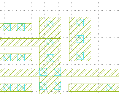
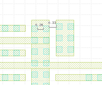
templayer via1large via1
        grow 180
        shrink 1095
        grow 915
        and via1
1 1 1
1