Guild icon
wafer.space Community
📐 - Designing / 🕰️-analog
Between 2026-03-31 11:59 p.m. and 2026-05-01 12:00 a.m.

Avatar
Are there instructions for linking xschem to the pdk symbol+schematic libraries and bsim models ?
1:40 a.m.
(or maybe the bsim models are more relevant to ngspice and or xyce)
Avatar
Avatar
nmz787
Are there instructions for linking xschem to the pdk symbol+schematic libraries and bsim models ?
If you haven't figured it out yet I'm happy to share my setup I got a lil help from tnt on with you if you'd write it into a brief blog post like "tutorial/instructions", like this weekend.
Avatar
In other "topic", how high-order of a delta-sigma DAC would be reasonable to pull off for on-die bias generation? I'd prefer to get by with a modest oversampling ratio to keep decent loop bandwidth even with the digital PLL being "limited" to CMOS logic speeds instead of the core's MCML (there's no way I finish enough of a cell library to make even just the delta sigma modulator (probably MASH?) out of MCML, before the deadline) speeds... It'd already look at doing the fast side of the time-to-digital converter in the little amount of MCML (as that way it would at least be able to directly count quarter clocks of timing, I think...).
Avatar
Avatar
namibj
If you haven't figured it out yet I'm happy to share my setup I got a lil help from tnt on with you if you'd write it into a brief blog post like "tutorial/instructions", like this weekend.
I would love to... But I'm on vacation away from laptop with my setup until Monday
7:06 p.m.
And no I didn't figure it out. I spent time trying to kick openAI codex to build something for me lol
Avatar
Avatar
nmz787
I would love to... But I'm on vacation away from laptop with my setup until Monday
wednesday daytime berlin time should work, probably
Avatar
Anyone happen to have some examples for "parametric cells" that try to do analog "buffer"/"amplifier"? I.... kinda need to quickly figure out how to automate layout-parasitics-including tuning so I can get it running. I have sufficiently-ish conquered xschem on the matter but that's ignorant of layout parasitics.
Avatar
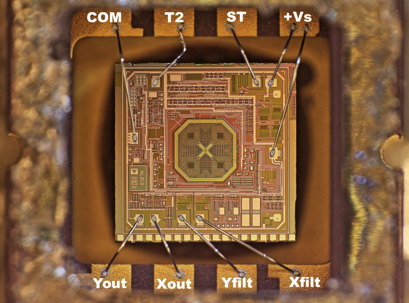
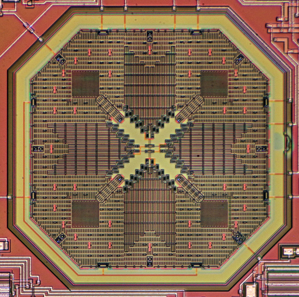
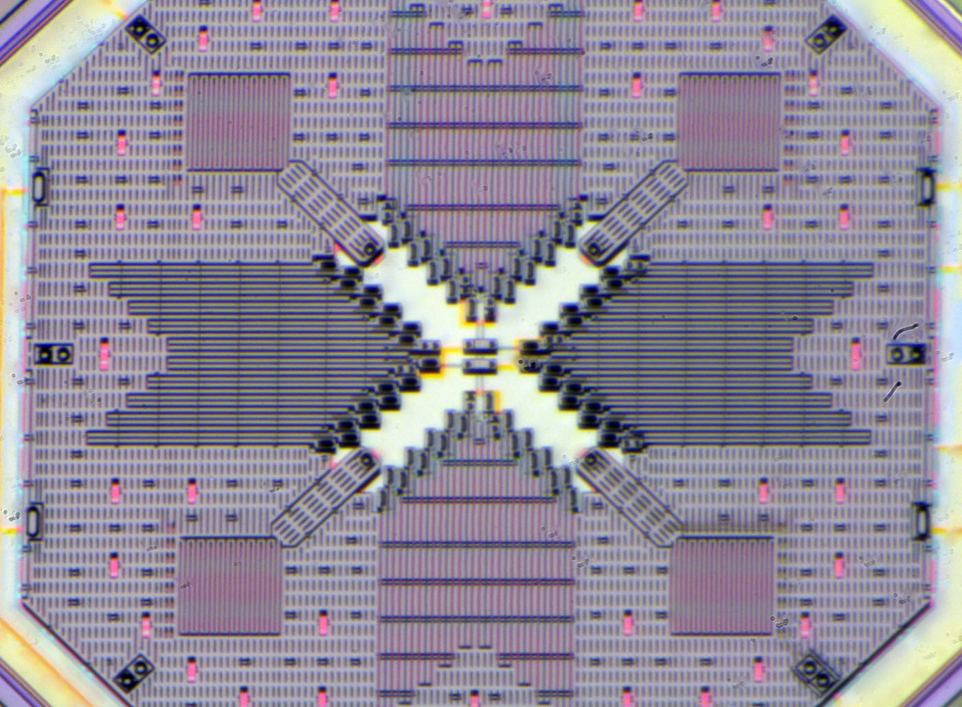
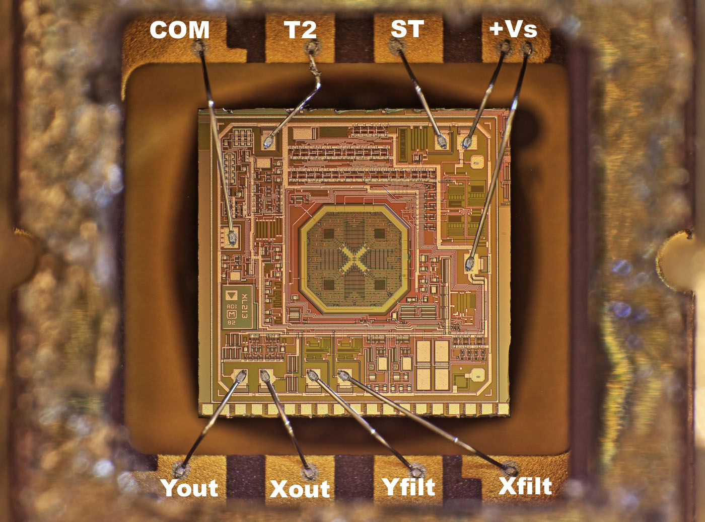
honest Q, is a MEMS device considered analog.?
6:32 a.m.
6:40 a.m.
i believe 'laser ablation' of the wafer to make thru-trenches after its been processed like regular silicon for the electronic parts, and before packaging, is the usual process , sometimes they are back-ground to make them thinner too.
Avatar
Avatar
Buzz
honest Q, is a MEMS device considered analog.?
Tim 'mithro' Ansell 2026-04-21 6:42 a.m.
Kinda but not really. MEMS generally requires things like undercuts which are not something supported on silicon process technologies - the circuits driving / reading the MEMS structures are frequently analog ADC/DACs. If you are interested in MEMS maybe check out science.xyz - they had credit card orderable MEMS processes.
Avatar
https://www.analog.com/en/resources/technical-articles/accelerometer-and-gyroscopes-sensors-operation-sensing-and-applications.html a mems gyro is usually in constant oscillation and a mems accelerometer is usually not, but they are fundamentally compatible technologies.
7:00 a.m.
its basically measuring capacitance change over time
7:01 a.m.
anyway, dont mine me, ive got a thing for sensors. 🙂
Avatar
Tim 'mithro' Ansell 2026-04-22 11:18 a.m.
Documentation for products and services by Science
Avatar
Ghaith Al Sabagh 2026-04-23 5:46 a.m.
I am not that expert, but this one seems to be like silicon technologies. https://science.xyz/docs/d/mems-soi/index IHP as far as I know offers LBE (localized backside etching) too.
Documentation for products and services by Science
Avatar
IHP does LBE but not on the cost reduced runs, you'll have to go through their full commercial service for that. (edited)
Avatar
Ghaith Al Sabagh 2026-04-23 5:48 a.m.
Actually it depends I think It is wafer post-processing
5:49 a.m.
You can still make a normal wafer on reduced cost, then send it to LBE
5:49 a.m.
I assume
Avatar
No, because on reduced cost the wafer is shared ... you don't get a full wafer 🙂
5:50 a.m.
Unless you can do LBE yourself on individual sliced dies.
5:50 a.m.
And LBE not being on the cost reduced runs is what IHP themselves said because that question was asked at some point.
Avatar
Ghaith Al Sabagh 2026-04-23 5:52 a.m.
The question is if an open-source community make a run for MEMS. Then they can share the wafer, but after LBE. What I mean is that It would be possible to handle such issue for a whole wafer after discussing with IHP. It would cost somehow more yes
Avatar
Tim 'mithro' Ansell 2026-04-23 5:53 a.m.
Could you potentially get wafers.space wafers LBE? I do offer purchase of full wafers.
Avatar
Ghaith Al Sabagh 2026-04-23 5:54 a.m.
Do you offer LBE?
Avatar
Avatar
Ghaith Al Sabagh
Do you offer LBE?
Tim 'mithro' Ansell 2026-04-23 2:21 p.m.
I do not.
Avatar
Joaquin Matres 2026-04-27 5:09 a.m.
For MEMs we have some open source structures here https://gdsfactory.github.io/gdsfactory/components.html#gdsfactory.components.mems.gear @namibj For amplifiers you can check out https://gdsfactory.github.io/IHP/cells.html
Avatar
I didn't realize gdsfactory had such a wide array of pcells!
Avatar
Thomas Pluck 2.1 2026-04-27 5:56 p.m.
So looks like Danube River is out of gas and we need someone to measure the test structures, anybody able and willing with a probe station to make it happen?
5:58 p.m.
(unless you're some kind of corporate shill)
Avatar
keyence enters chat
Avatar
Thomas Pluck 2.1 2026-04-27 6:34 p.m.
Avatar
Avatar
BreakingTaps
keyence enters chat
looks at beloved https://www.iptest.com/ mousepad
The fastest power discrete semiconductor testers for MOSFET, IGBT, SiC and GaN. Perform static, switching, thermal and avalanche energy tests at high speeds.
Avatar
Avatar
Thomas Pluck 2.1
So looks like Danube River is out of gas and we need someone to measure the test structures, anybody able and willing with a probe station to make it happen?
Tim 'mithro' Ansell 2026-04-28 7:30 a.m.
Probably out of our price range, but CoolCAD did a bunch of the testing for the SKY130 raw data repo in conjunction with NIST.
Avatar
Avatar
BreakingTaps
Been dabbling with analog recently and was curiosu if any of the automated analog layout tools worked well. ALIGN (https://github.com/ALIGN-analoglayout/ALIGN-public) looked most promising and had a Sky130 PDK, so I threw Claude Code at it. Sorta have a working GF180 PDK now? Takes in a spice netlist, constraints (matching, symmetry, etc) and spits out GDS Found some pretty serious limitations though, namely that ALIGN was built with finfet nodes in mind so there are a lot of restrictive routing/placement constraints baked into the core. Had to modify the core to get even moderately compact layouts and it's still a lot of wasted space. DRC and LVS match, but haven't run simulations on the generated output yet... could be hot garbage 😅 Still, neato tool. Kinda want to start working on something that's tailored for big legacy nodes that have less restrictive DRC. (screenshot is a CSA + Discriminator + Krummenacher feedback circuit that i've been playing around with)
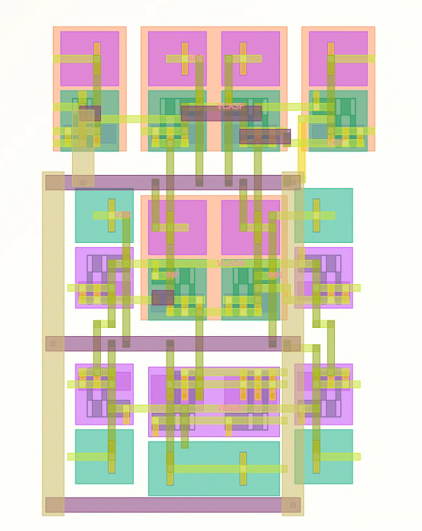
still poking at my GF180 pdk for ALIGN. starting to see light at the end of the tunnel, most (synthetic) generated designs are coming out LVS and DRC clean. Still needs some human sanity checking to make sure the schematics are what they are actually supposed to be. But from just skimming designs they are looking better than before, respecting constraints like symmetry now, etc
ferrisCatOwO 1
7:14 p.m.
still some issues with spacing but it's a constant battle against overzealous packing and DRC violations 🫠
Avatar
Avatar
BreakingTaps
still poking at my GF180 pdk for ALIGN. starting to see light at the end of the tunnel, most (synthetic) generated designs are coming out LVS and DRC clean. Still needs some human sanity checking to make sure the schematics are what they are actually supposed to be. But from just skimming designs they are looking better than before, respecting constraints like symmetry now, etc
Tim 'mithro' Ansell 2026-04-29 12:02 a.m.
When you say ALIGN - do you mean the project that came out of the DARPA IDEA/POSH program?
Avatar
Avatar
Tim 'mithro' Ansell
When you say ALIGN - do you mean the project that came out of the DARPA IDEA/POSH program?
Contribute to ALIGN-analoglayout/ALIGN-public development by creating an account on GitHub.
12:14 a.m.
(yes seems to be from that DARPA IDEA/ERI "no humans in the loop" project)
Avatar
Tim 'mithro' Ansell 2026-04-29 12:17 a.m.
Yeap!
12:18 a.m.
@BreakingTaps - We should most certainly send GF180MCU support upstream if you get it working.
12:18 a.m.
@BreakingTaps - I met the people behind ALIGN a few times at the DARPA workshops.
Avatar
will try to tidy things up when I get everything in working order! I did make some changes to ALIGN itself which may be difficult to upstream but we can have a chat with them. There are a number of assumptions baked into how it places cells, mostly assuming you're on a finfet node. So it standardizes row height, adds dummy poly fingers after cells, stuff like that. Ended up wasting a ton of space on a big node like GF180 Loosening some of those rules then puts cells in potential corner-contact between rows, so added some constraints to the ILP solver to avoid corner touches etc etc
2:03 a.m.
that said, I think the GF180 PDK itself should be portable to "stock" ALIGN, it'll just be bulky
Avatar
Tim 'mithro' Ansell 2026-04-29 6:20 a.m.
@BreakingTaps - They have some demonstration bulk node PDKs (edited)
Avatar
yeah there's a sky130 in there. i haven't looked at it for a while but iirc it also had a ton of wasted space
Avatar
The biggest problem was multiple dummy fingers get appended to edges of cells. The hardcoded values in ALIGN uses gateDummy=3, which adds 3.2um per cell of "wasted" poly strips per cell (multiplied by the number of xcells the transistor is being split into). Cells are also rounded to multiples of M3 pitch (800nm) which can interact badly with the finger widths too and bulk it even more Row heights are pinned to the tallest cell, so you can also get big empty rows despite the solver trying to minimize area. None of it is _wrong per se, but it's definitely optimized for a node that has discrete diffusion/fin widths and tight gate pitches (at least from my outsider, relative newcomer 🙂 ) (edited)
4:36 p.m.
but luckily, open source! so easy enough to tweak and experiment with 🙂
Avatar
Avatar
BreakingTaps
still poking at my GF180 pdk for ALIGN. starting to see light at the end of the tunnel, most (synthetic) generated designs are coming out LVS and DRC clean. Still needs some human sanity checking to make sure the schematics are what they are actually supposed to be. But from just skimming designs they are looking better than before, respecting constraints like symmetry now, etc
got a schematic to go wtih that layout by chance?
Avatar
Avatar
namibj
got a schematic to go wtih that layout by chance?
Believe it was this one. Caveat that this schematic was synthetically generated and very possibly nonsensical 🙂 * Folded Cascode OTA: W=1.32u, NF=2 .SUBCKT OTA_FOLDED_W1P32U_NF2 VSS VDD INP INN OUT VBIAS VCASN VCASP * PMOS input differential pair M1 N1 INP TAIL VDD pfet_03v3 w=1.32u l=280n nf=2 m=1 M2 N2 INN TAIL VDD pfet_03v3 w=1.32u l=280n nf=2 m=1 * Tail current source M0 TAIL VBIAS VSS VSS nfet_03v3 w=2.64u l=280n nf=2 m=2 * Folded NMOS cascode M3 N1 VCASN N3 VSS nfet_03v3 w=1.32u l=280n nf=2 m=1 M4 N2 VCASN N4 VSS nfet_03v3 w=1.32u l=280n nf=2 m=1 * NMOS current source M9 N3 VBIAS VSS VSS nfet_03v3 w=1.32u l=280n nf=2 m=1 M10 N4 VBIAS VSS VSS nfet_03v3 w=1.32u l=280n nf=2 m=1 * PMOS cascode loads M5 N1 VCASP N5 VDD pfet_03v3 w=1.32u l=280n nf=2 m=1 M6 N5 N5 VDD VDD pfet_03v3 w=1.32u l=280n nf=2 m=1 M7 N2 VCASP OUT VDD pfet_03v3 w=1.32u l=280n nf=2 m=1 M8 OUT N5 VDD VDD pfet_03v3 w=1.32u l=280n nf=2 m=1 .ENDS OTA_FOLDED_W1P32U_NF2
Avatar
as long as it reasonably confidently corresponds to the layout I'm fine
Avatar
(there's also a constraint file that goes along with that somewhere, which specifies stuff like symmetry. would need to hunt for that when i get home)
Avatar
i'd happily take a "fresh" pair btw if that's easier to givew with confidence
11:26 p.m.
oh I'm going to bed now, they took my teeth yesterday 🙁
Avatar
😩 oof, feel better!
11:27 p.m.
I'd expect to look at things now sooner than 20 hours from now fyi
Avatar
Tim 'mithro' Ansell 2026-04-30 3:19 a.m.
@BreakingTaps - IIRC The ALIGN team had outstanding success with FinFET nodes due to the very limited type of transistors that you are allowed on them and then struggled with extending it back to planar technologies.
👍 1
Avatar
ahh interesting. that makes sense, tracks with the sorts of limitations i'm seeing. on the upside, claude/codex are helping me beat back the edge cases by just throwing tons of samples at it and iterating on failures. bit tedious but making progress
Avatar
Tim 'mithro' Ansell 2026-04-30 9:34 a.m.
"bit tedious but making progress" I think describe all software development a lot of the time 😉
😁 1
Avatar
Avatar
Tim 'mithro' Ansell
Probably out of our price range, but CoolCAD did a bunch of the testing for the SKY130 raw data repo in conjunction with NIST.
Thomas Pluck 2.1 2026-04-30 2:04 p.m.
Welp, that one's dead on arrival - hope there's something left on Run 2 to get this done for real without ideological strings attached
Avatar
huh? ideological strings attached?
2:26 p.m.
feel like I'm missing a ton of context here 😄
Avatar
Tim 'mithro' Ansell 2026-04-30 3:09 p.m.
@BreakingTaps - @Thomas Pluck 2.1 was offering to figure out characterization of existing test structures taped out on the GF180MCU process technology (see https://siliconpr0n.org/archive/doku.php?id=mcmaster:efabless:gf180mcu-mpw18h1-18100001&s[]=gf180mcu) -- The idea that having some data from these structures would mean better/more advanced ones could then be created for Run #2 and allow even better understanding of the process technology. Sadly the people who currently possess the die are unwilling to share them.
👍 2
Avatar
ahh, booo 🙁
ferrisCatPensive 3
Exported 69 message(s)
Timezone: UTC+0