Guild icon
wafer.space Community
📐 - Designing / 📦-cob
Channel for discussing chip-on-board packaging options for wafer.space bare die.
Between 2025-10-31 11:59 p.m. and 2025-12-01 12:00 a.m.

Avatar
NIST lets you rent dicing saws and wire bonders by the hour. So does RPI in Troy, NY.
👍 1
Avatar
Avatar
Mark Anderson
NIST lets you rent dicing saws and wire bonders by the hour. So does RPI in Troy, NY.
Tim 'mithro' Ansell 2025-11-04 12:02 a.m.
@Andrew Wingate / @carlfk -^
Avatar
So the https://github.com/wafer-space/chip-on-board-wire-bonded-pcbs repository talks about "default" designs that must share the wirebonding layout, PCB size (14mm x 16mm), connector location (if present). Is the implication here that the crowd supply run will allow one to provide their own design that fits those constraints or is it expected that there will be one specific layout selected to be used by all COB orders?
Avatar
Tim 'mithro' Ansell 2025-11-04 12:34 a.m.
@Brian Swetland - The expectation is that a number of designs will be selected as supported by the crowd supply run.
Avatar
Avatar
Tim 'mithro' Ansell
@Andrew Wingate / @carlfk -^
Andrew Wingate 2025-11-04 1:13 a.m.
I did see that. Where is NIST?
Avatar
Tim 'mithro' Ansell 2025-11-04 1:14 a.m.
No idea 🙂
Avatar
Leo Moser (mole99) 2025-11-07 11:41 a.m.
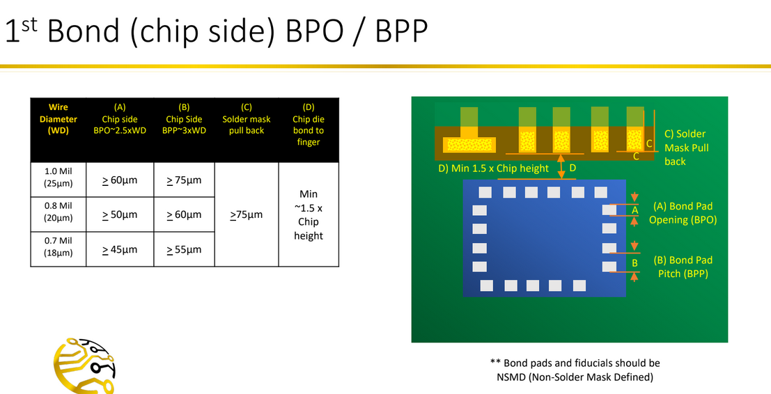
@Tim 'mithro' Ansell @Andrew Wingate Could you please tell me what the minimum spacing between the bondpads is for CoB packaging? The bondpads are 60µm x 60µm.
Avatar
Avatar
Leo Moser (mole99)
@Tim 'mithro' Ansell @Andrew Wingate Could you please tell me what the minimum spacing between the bondpads is for CoB packaging? The bondpads are 60µm x 60µm.
Are you talking about the PCB? Or the die?
Avatar
Leo Moser (mole99) 2025-11-07 11:42 a.m.
About the die.
Avatar
I really have no idea other than the document Tim sent me. https://drive.google.com/file/d/1touEQHWAOTon_98TdiVLKKqsQ8RJJ1tP/view Looks like 15µm between pads
Avatar
Avatar
Andrew Wingate
I really have no idea other than the document Tim sent me. https://drive.google.com/file/d/1touEQHWAOTon_98TdiVLKKqsQ8RJJ1tP/view Looks like 15µm between pads
Leo Moser (mole99) 2025-11-07 11:49 a.m.
Thanks! That's much better than I had expected. @Tim 'mithro' Ansell can you confirm?
👍 1
Avatar
Avatar
Andrew Wingate
I really have no idea other than the document Tim sent me. https://drive.google.com/file/d/1touEQHWAOTon_98TdiVLKKqsQ8RJJ1tP/view Looks like 15µm between pads
Tim 'mithro' Ansell 2025-11-07 11:52 a.m.
Weren't you going to bed? 😛
😭 1
Avatar
Avatar
Leo Moser (mole99)
Thanks! That's much better than I had expected. @Tim 'mithro' Ansell can you confirm?
Tim 'mithro' Ansell 2025-11-07 11:53 a.m.
I don't have any actual specs from the Chinese vendors at the moment -- the more spacing we can get the better I think? @stuart - What are the requirements for your vendor?
Avatar
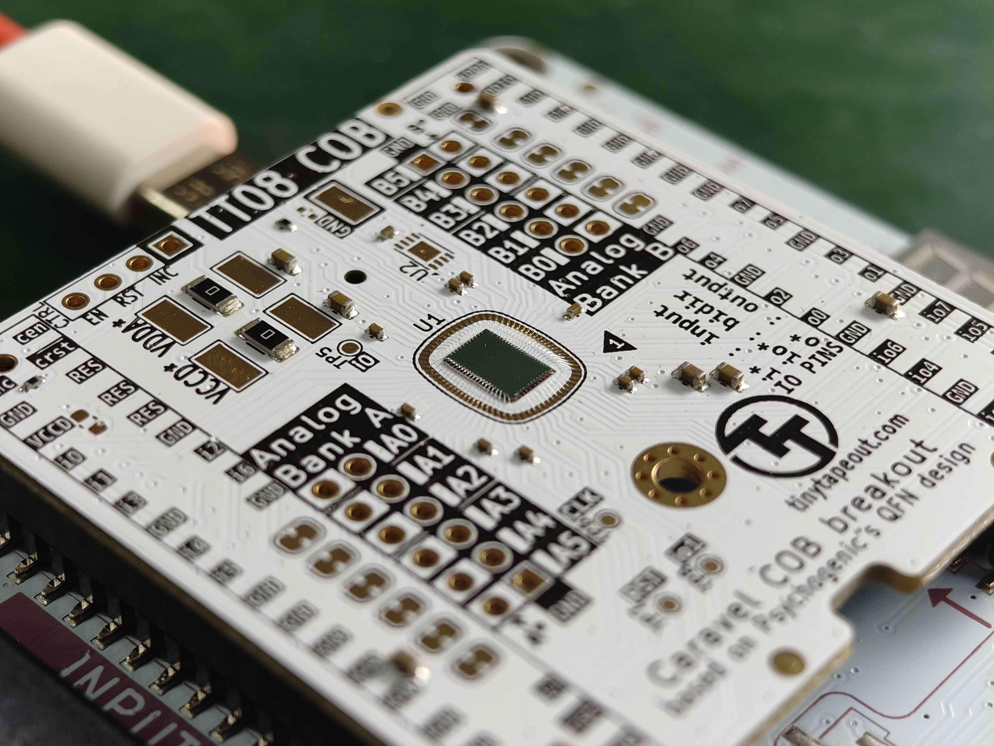
@stuart 's doing some TT COB today, and I wanted to share this lovely photo!
❤️ 7
😍 3
Avatar
looks nice! is that by manual wirebonder or programmed?
Avatar
Programmed, we'll be sharing some more photos and info about the process soon 🦋
3:32 p.m.
3:32 p.m.
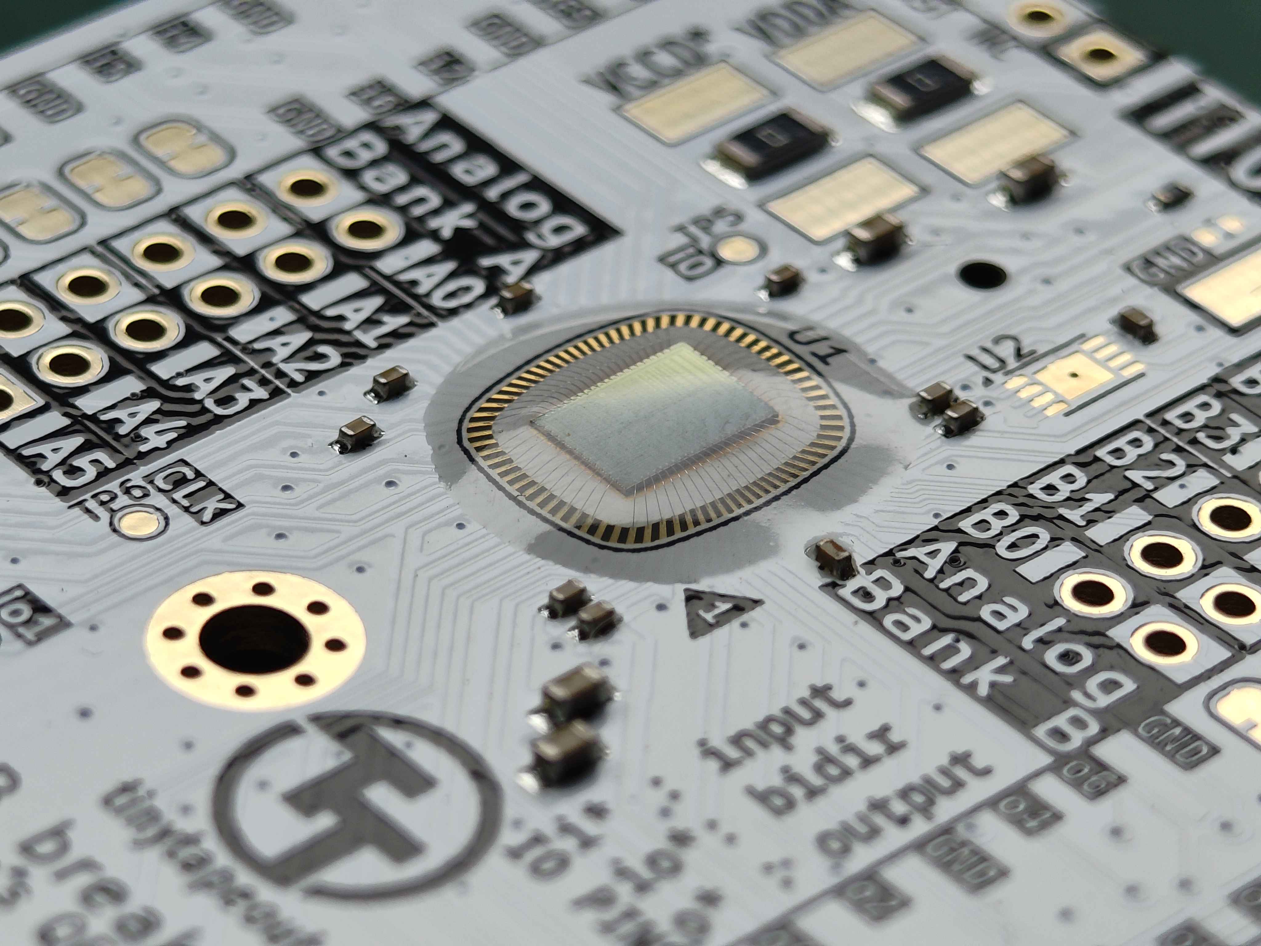
Here's one post-glob
Avatar
programmed is the dream. I've assembled a lot of parts with a west-bond but someday I hope to find an affordable programmable bonder
Avatar
Avatar
stuart
Programmed, we'll be sharing some more photos and info about the process soon 🦋
Yes, please share! I need to learn more about wire bonding if I wanna be able to bond my own chips one day soon.
Avatar
Avatar
stuart
Click to see attachment 🖼️
Tim 'mithro' Ansell 2025-11-14 9:41 p.m.
Who's padring and die is that?
Avatar
@Tim 'mithro' Ansell It's TT08, sky130 default pad ring.
Avatar
Tim 'mithro' Ansell 2025-11-14 10:08 p.m.
I guess I actually ment the cob ring
Avatar
ReJ aka Renaldas Zioma 2025-11-21 4:37 p.m.
Hello, I am really late to the party, just finished reading the channel contents. On the plus side Z80 is all dandy and passing prechecks without violations. Similar to @Tholin I am interested in the DIP PCB. DIP is for Z80. That means only 40 pins all digital 5V. Classical DIP40. My preferences: 1) first would be small LGN pcb as long as it can be soldered onto DIP PCB without destroying the wirebonding. 2) second would be binding chip directly to DIP40 PCB where I can route GND (to pin 29) and VDD (to pin 11 of the DIP40). Mezzanine - while very flexible I am worried that it would make the final package look "weird" and too high, also I still not sure what would that mean to the final cost. So for Z80 I would say it as a Plan C. Just to clarify, is LGN option still on the table? (edited)
Avatar
On a PCB, you can route any pad on the COB footprint to any pin on the headers - that’s no problem. I am trying to keep compatibility with DIP-40 ceramic carriers where those connections are fixed.
4:38 p.m.
So I had to move around some VDD/VSS pads
4:39 p.m.
And can thus no longer use the mezzanine breakout as it makes assumptions about the locations of the ground pads and wires them all to a ground plane. (edited)
4:39 p.m.
So, I’m also interested in other options.
Avatar
Avatar
Tholin
So I had to move around some VDD/VSS pads
ReJ aka Renaldas Zioma 2025-11-21 4:40 p.m.
Just to clarify VDD/VSS pads - you had to move them on the chip ring layout or outside (on PCB)?
Avatar
The chip ring layout
👍 1
Avatar
Avatar
Tholin
On a PCB, you can route any pad on the COB footprint to any pin on the headers - that’s no problem. I am trying to keep compatibility with DIP-40 ceramic carriers where those connections are fixed.
ReJ aka Renaldas Zioma 2025-11-21 4:47 p.m.
I looked at your reference to DIP-40 ceramic carrier and I wonder how did they managed to put Z80 in ceramic back in the day, because they have VDD/GND not on 40/20 pins. Did they have special ceramic packages for them? (unfortunately I don't have Z80 in ceramic for inspection)
Avatar
The ceramic carrier makes no assumptions about the location of the power pins. It simply breaks the 40 pins out to 40 bonding pads.
4:49 p.m.
There is a metal plane at the base of the cavity, but you have to bond it to the ground pin yourself by running a wire from the carrier’s bond bad to the plane.
4:49 p.m.
At least, that is how I understand it.
4:49 p.m.
But I still had to customize my die’s padring since I am replicating existing chips and thus need specific ground/power connections.
Avatar
Avatar
Tholin
But I still had to customize my die’s padring since I am replicating existing chips and thus need specific ground/power connections.
ReJ aka Renaldas Zioma 2025-11-21 4:54 p.m.
OK, I think I understood what you are saying. Ceramic unlike PCB enforces a very strict wiring between the padring and DIP pins. So you have to match the pin locations to the original chip essentially.
Avatar
Yes. And now I can’t use the mezzanine breakout because it assumes that the ground pads are in specific locations.
Avatar
ReJ aka Renaldas Zioma 2025-11-21 4:55 p.m.
Yes, makes sense.
Avatar
This could technically be solved by creating a "dumb" version of that breakout that just routes each pad to a pin on the mezzanine without making any assumptions, with the PCB ground plane unconnected to any chip pads and routed to a spare mezzanine pin. This I could use for prototyping, as long as I also still get raw dies for my ceramic carrier experiments!
👍 1
4:57 p.m.
But ultimately, I resigned myself to coming up with my own solution.
Avatar
ReJ aka Renaldas Zioma 2025-11-21 5:13 p.m.
For LGN option, I also wonder, if it would be possible to have a narrower LGN board? (while keeping bonding pattern in the same way as “normal” LGN if it reduced the price / headache. Some internal pads would simply left unconnected for some pads) (edited)
5:13 p.m.
Sorry for extremely crude art
5:13 p.m.
5:17 p.m.
The reasoning here is that it might not fit on DIP otherwise. Classic DIP has less than 14 mm on the top and “fake” PCB DIPs might have protruding pins from below
5:17 p.m.
Avatar
Avatar
Tholin
This could technically be solved by creating a "dumb" version of that breakout that just routes each pad to a pin on the mezzanine without making any assumptions, with the PCB ground plane unconnected to any chip pads and routed to a spare mezzanine pin. This I could use for prototyping, as long as I also still get raw dies for my ceramic carrier experiments!
Andrew Wingate 2025-11-21 7:52 p.m.
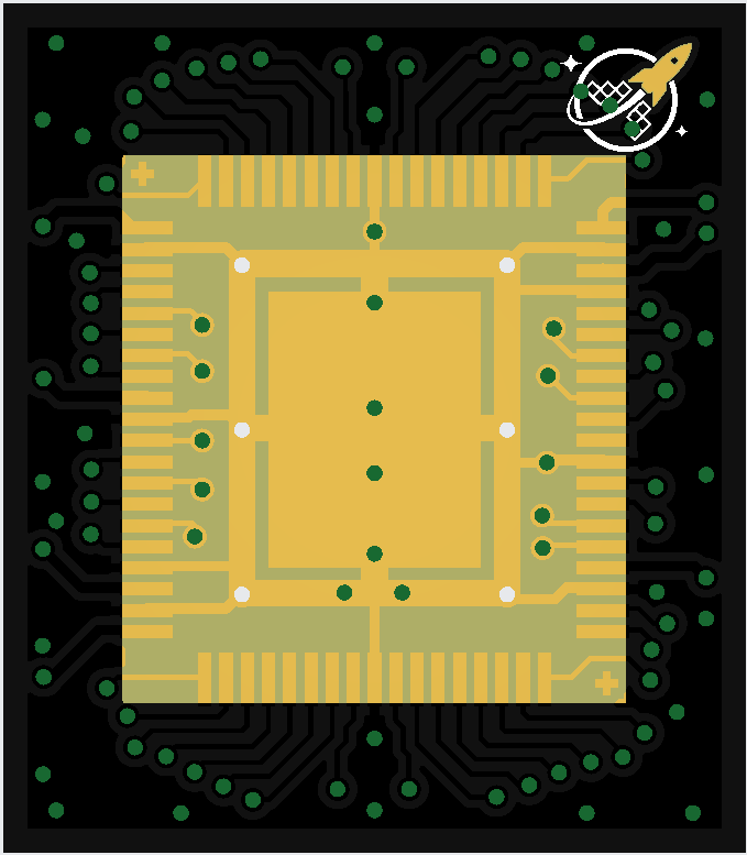
I will be taking one more pass at the cob PCB, I will try to be more amenable to changes with this revision. Ultimately there are more pins on the die than there are on the mezzanine, so there will be some considerations needed there. Afaik we still have not had any real conversations with wirebonders so are still not sure on what they are willing to accept for deviations from the norm. I still think that as long as bonding locations and overall form factor remain constant we should be able to have a lot of variations.
Avatar
Avatar
ReJ aka Renaldas Zioma
For LGN option, I also wonder, if it would be possible to have a narrower LGN board? (while keeping bonding pattern in the same way as “normal” LGN if it reduced the price / headache. Some internal pads would simply left unconnected for some pads) (edited)
Andrew Wingate 2025-11-21 8:00 p.m.
The LGA version is temporarily abandoned given concerns over reflowing and types of epoxies after wirebonding. I have also ordered some 50pin mezzanine connectors to play with for a lower pin count version. The cost for these connectors is quite affordable even at quantity. https://www.lcsc.com/product-detail/C2763977.html
Avatar
Avatar
Andrew Wingate
The LGA version is temporarily abandoned given concerns over reflowing and types of epoxies after wirebonding. I have also ordered some 50pin mezzanine connectors to play with for a lower pin count version. The cost for these connectors is quite affordable even at quantity. https://www.lcsc.com/product-detail/C2763977.html
ReJ aka Renaldas Zioma 2025-11-21 8:41 p.m.
Is there a prototype bonding plan for 50pin mezzanine connector somewhere I could take a look? I think I only found a 70pin version in the repo.
Avatar
Avatar
ReJ aka Renaldas Zioma
Is there a prototype bonding plan for 50pin mezzanine connector somewhere I could take a look? I think I only found a 70pin version in the repo.
Andrew Wingate 2025-11-21 8:41 p.m.
Sorry, no, It's just something I've been talking about doing.
8:42 p.m.
There is no padring yet, so not sure what anything will look like.
Avatar
ReJ aka Renaldas Zioma 2025-11-21 8:45 p.m.
For retro DIP40 I am gravitating to use primarily North and South side (32 pins) of the padring and the rest put as close to the corner as possible. Dunno if that might be a stupid idea? The reasoning is to keep sides as empty as possible in case LGA comes back and I could keep it narrow.
8:48 p.m.
Would / could that be compatible with 50pin mezzanine layout you are thinking about?
Avatar
Avatar
ReJ aka Renaldas Zioma
For retro DIP40 I am gravitating to use primarily North and South side (32 pins) of the padring and the rest put as close to the corner as possible. Dunno if that might be a stupid idea? The reasoning is to keep sides as empty as possible in case LGA comes back and I could keep it narrow.
Andrew Wingate 2025-11-21 8:55 p.m.
That sounds close to what I had in mind. Like I said above to @Tholin I think for now the safest bet could be to consider this a subset of the standard wirebonding frame. I have ordered the board you see posted here and I'll be taking another pass at it and probably be shrinking some parts making the whole thing more narrow. Also hopefully soon we will have open dialogs with wirebonders and we'll get a lot more info about what's best/possible/etc.
Avatar
Avatar
Andrew Wingate
That sounds close to what I had in mind. Like I said above to @Tholin I think for now the safest bet could be to consider this a subset of the standard wirebonding frame. I have ordered the board you see posted here and I'll be taking another pass at it and probably be shrinking some parts making the whole thing more narrow. Also hopefully soon we will have open dialogs with wirebonders and we'll get a lot more info about what's best/possible/etc.
ReJ aka Renaldas Zioma 2025-11-21 9:22 p.m.
Could you explain why do you say that it is a subset of a wirebonding scheme? I think I see all the pads from the chip pad frame (at least @Leo Moser (mole99)’s template) exposed and bondable. I am I missing something?
Avatar
Avatar
ReJ aka Renaldas Zioma
Could you explain why do you say that it is a subset of a wirebonding scheme? I think I see all the pads from the chip pad frame (at least @Leo Moser (mole99)’s template) exposed and bondable. I am I missing something?
Andrew Wingate 2025-11-21 9:30 p.m.
I mean (and this is still my opinion only) that toolchains could remain more simple if we only change a few things at a time with the wirebonders, so the wirebonding frame would still have bonds at the same locations. Again, I don't know a lot of things, and what constitutes different as far as their pattern matching and other toolchains consider the same or not. With the deadline looming, I don't know how many variations there will be in this run. But will try to keep everyone updated as I go along.
👍 1
Avatar
ReJ aka Renaldas Zioma 2025-11-22 8:39 a.m.
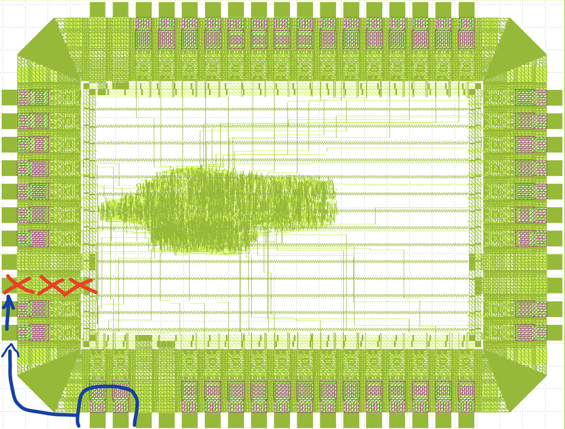
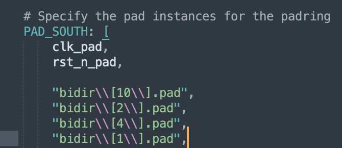
@Leo Moser (mole99) what is more advisable & future proof when defining the mapping between the core signals and pads on a padring? Imagine I have 16-bit address bus of the retro chip and I want to assign them to a particular physical pads, should I better a) change the binding order in config.yaml modifying PAD_SOUTH,PAD_EAST ... NOT changing power pad locations! Those stay always the same as in the template. (edited)
8:39 a.m.
8:42 a.m.
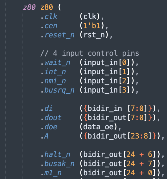
or b) only change how it is defined in Verilog file, say in chip_core.sv, but never touch config.yaml PADs
8:42 a.m.
Avatar
Avatar
ReJ aka Renaldas Zioma
@Leo Moser (mole99) what is more advisable & future proof when defining the mapping between the core signals and pads on a padring? Imagine I have 16-bit address bus of the retro chip and I want to assign them to a particular physical pads, should I better a) change the binding order in config.yaml modifying PAD_SOUTH,PAD_EAST ... NOT changing power pad locations! Those stay always the same as in the template. (edited)
Leo Moser (mole99) 2025-11-22 11:20 a.m.
Hi ReJ! I'm not sure what you mean by "future proof". Do you mean in regards to code changes to the template? The easier way is to change it in the RTL, as you only need to connect your signals to the bidir vector. However, it may be confusing to keep track of all the signals in bidir. That's why I think the better apporach would be to make another generate loop that instantiates the pads for the address bus and give it a better name than bidir, e.g. addr_bus. You would then need to reduce the number of bidir pins accordingly. Finally, you can add the addr_bus\\[x\\].pad instances to the yaml (and remove some of the bidir instances). Unfortunately, when the upstream template changes, this approach may lead to more conflicts.
Avatar
Avatar
Leo Moser (mole99)
Hi ReJ! I'm not sure what you mean by "future proof". Do you mean in regards to code changes to the template? The easier way is to change it in the RTL, as you only need to connect your signals to the bidir vector. However, it may be confusing to keep track of all the signals in bidir. That's why I think the better apporach would be to make another generate loop that instantiates the pads for the address bus and give it a better name than bidir, e.g. addr_bus. You would then need to reduce the number of bidir pins accordingly. Finally, you can add the addr_bus\\[x\\].pad instances to the yaml (and remove some of the bidir instances). Unfortunately, when the upstream template changes, this approach may lead to more conflicts.
ReJ aka Renaldas Zioma 2025-11-22 12:55 p.m.
TBH, I am mostly worried that if touch something in config.yaml the pad's physical locations will change 😓 maybe an unfound fear (edited)
Avatar
I did update my pad config (here https://github.com/Wren6991/RISCBoy-180/blob/b3dc3bb41600123395ae37ca25f37694c35ff448/librelane/config.yaml#L150-L260) and left in lots of comments for the fixed locations of the VDD/VSS pads. Still quite paranoid and it's on my list of things to re-check before submission, but I thought this was less painful overall because I can use the correct pad names in IO constraints etc.
Games console SoC for GF180MCU process. Contribute to Wren6991/RISCBoy-180 development by creating an account on GitHub.
1:19 p.m.
Are there any automated checks for VDD/VSS locations remaining compatible with the COB breakout?
❤️ 1
Avatar
Avatar
ReJ aka Renaldas Zioma
TBH, I am mostly worried that if touch something in config.yaml the pad's physical locations will change 😓 maybe an unfound fear (edited)
Leo Moser (mole99) 2025-11-22 1:47 p.m.
As long as you keep the same number of pads on each side, you will be fine :) All of the I/O pads in gf180mcu are the same width. So, when LibreLane places them equidistant from each other, you will always get the same bondpad loactions.
👍 1
Avatar
Avatar
LukeW
Are there any automated checks for VDD/VSS locations remaining compatible with the COB breakout?
Leo Moser (mole99) 2025-11-22 1:50 p.m.
There aren't any checks for that yet. I could add one based on the XOR of the pad layer. However, this would probably only be for the second shuttle, as it requires information from the online platform on whether the user has selected the CoB option or not.
1:54 p.m.
If you mean checking whether there are actual VDD/VSS cells at these locations. This would require checking the cells themselves, which would be impratical. Someone could do a custom design which uses a different kind of power/ground cells.
Avatar
Ok, I'll do a "manual DRC" for this run 😄
👌 1
Avatar
ReJ aka Renaldas Zioma 2025-11-23 10:52 a.m.
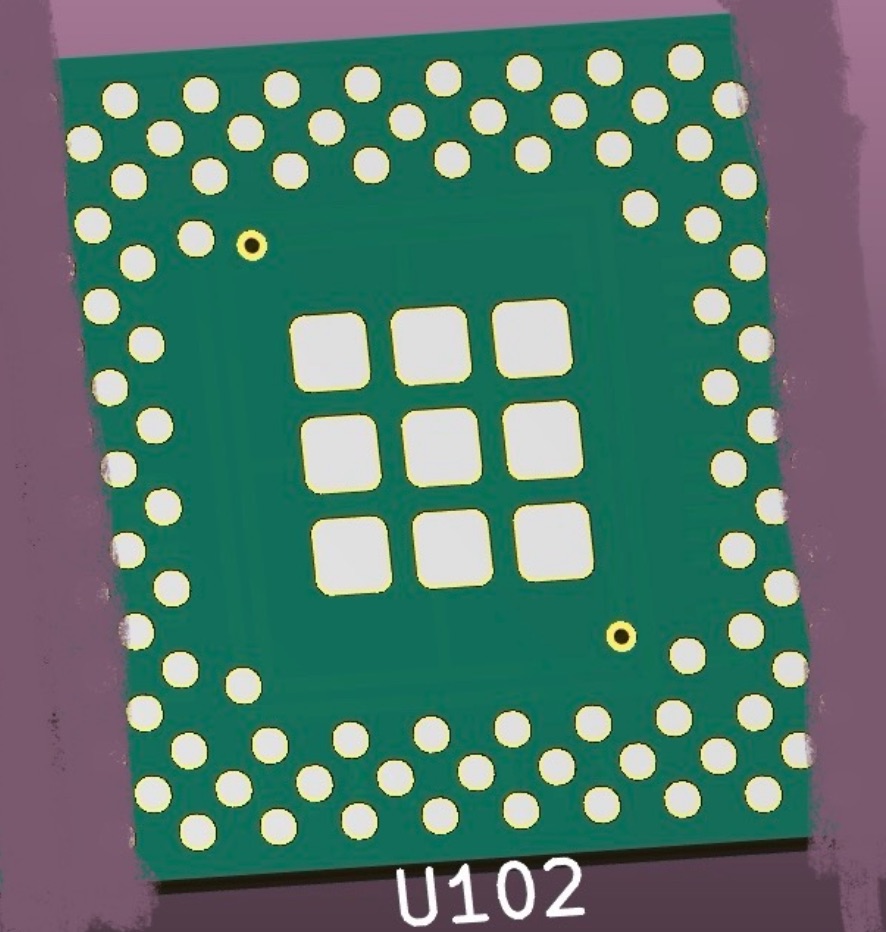
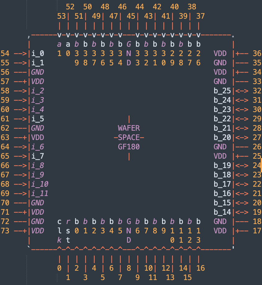
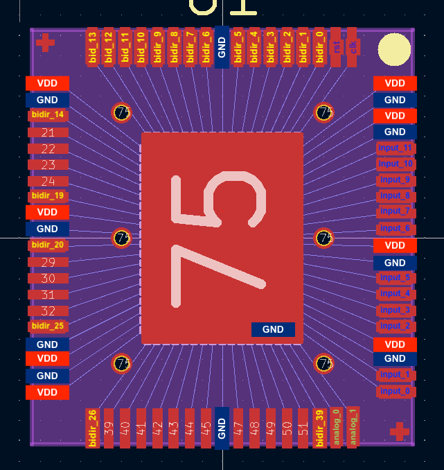
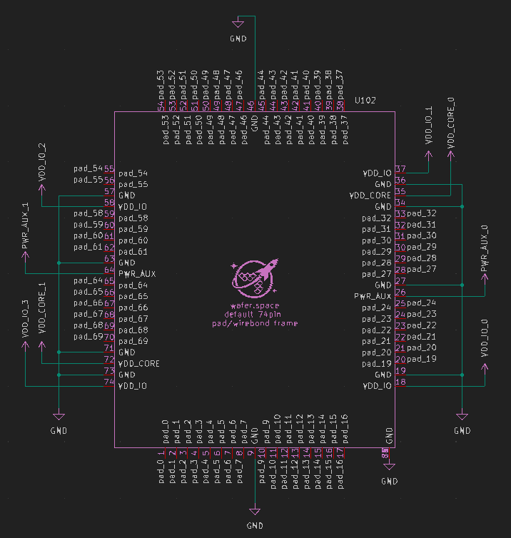
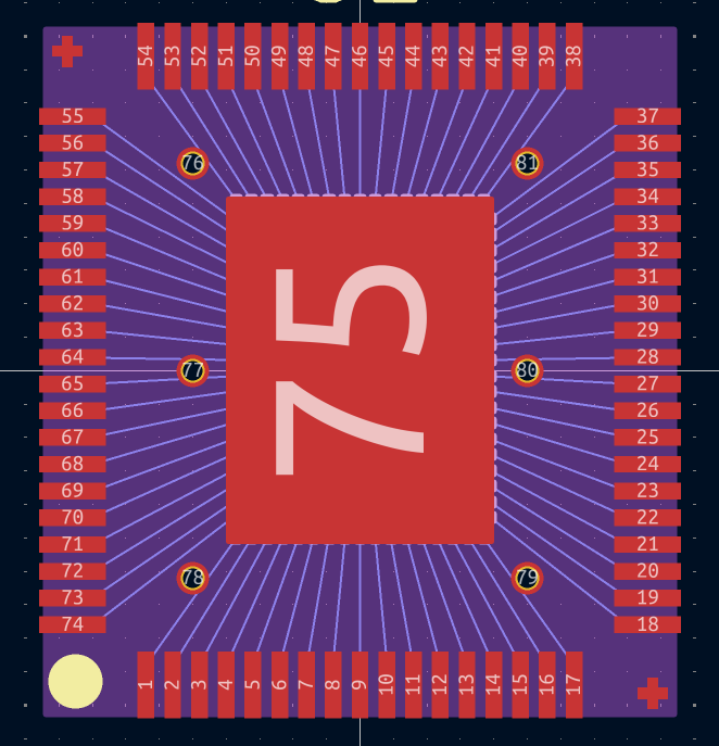
Please excuse my ASCII art, but I am struggling to map the names from the https://github.com/wafer-space/gf180mcu-project-template to the https://github.com/wafer-space/chip-on-board-wire-bonded-pcbs
10:52 a.m.
52 50 48 46 44 42 40 38 53| 51| 49| 47| 45| 43| 41| 39| 37 | | | | | | | | | | | | | | | | | ,------v-v-v-v-v-v-v-v---v-v-v-v-v-v-v-v-------. | a a b b b b b b G b b b b b b b b | 54 -->|i_0 1 0 3 3 3 3 3 3 N 3 3 3 3 2 2 2 2 VDD |+-- 36 55 -->|i_1 9 8 7 6 5 4 D 3 2 1 0 9 8 7 6 GND |--- 35 56 ---|GND VDD |+-- 34 57 --+|VDD GND |--- 33 58 -->|i_2 b_25|<-> 32 59 -->|i_3 b_24|<-> 31 60 -->|i_4 b_23|<-> 30 61 -->|i_5 | b_22|<-> 29 62 ---|GND WAFER b_21|<-> 28 63 --+|VDD -SPACE- b_20|<-> 27 64 -->|i_6 GF180 GND |--- 26 65 -->|i_7 | VDD |+-- 25 66 -->|i_8 b_19|<-> 24 67 -->|i_9 b_18|<-> 23 68 -->|i_10 b_17|<-> 22 69 -->|i_11 b_16|<-> 21 70 ---|GND b_15|<-> 20 71 --+|VDD b_14|<-> 19 72 ---|GND c r b b b b b b G b b b b b b b b GND |--- 18 73 --+|VDD l s 0 1 2 3 4 5 N 6 7 8 9 1 1 1 1 VDD |+-- 17 | k t D 0 1 2 3 | `------^-^-^-^-^-^-^-^---^-^-^-^-^-^-^-^-------' | | | | | | | | | | | | | | | | | 0 | 2 | 4 | 6 | 8 | 10| 12| 14| 16 1 3 5 7 9 11 13 15 Is this reasonable? (edited)
10:55 a.m.
i_0 .. i_11 input_PADs b_0 .. b_39 bidir_PADs a_0, a_1 analog_PADs based on the template default configuration
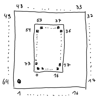
10:56 a.m.
@Andrew Wingate , @Leo Moser (mole99) could you please validate if I didn't screw up the orientation here?
Avatar
pad 0 is what you called pad 20 on the drawing above. But the position of power pads seems to match at least.
Avatar
Avatar
ReJ aka Renaldas Zioma
@Andrew Wingate , @Leo Moser (mole99) could you please validate if I didn't screw up the orientation here?
You unfortunately did. You made the same mistake I did when I was originally trying to unwind all this. I will continue to push that something similar to what you have here should be the standard, but the way it is now is that pin 0 is at the bottom left and then goes counterclockwise. I have a spreadsheet here that may help you to unwind it. https://docs.google.com/spreadsheets/d/1pI2BAEWEexXcXN3vah3SR85zPIV6eAXPGXc2bcvoSGU/edit?gid=0#gid=0 My brain thinks it's backwards as well
🙏 1
Avatar
ReJ aka Renaldas Zioma 2025-11-23 11:06 a.m.
fixing
Avatar
ReJ aka Renaldas Zioma 2025-11-23 11:13 a.m.
11:14 a.m.
@Andrew Wingate thanks for adding template pin names in that spreadsheet! That's very helpful!
Avatar
I'm trying to but things are still backwards..... ugh...
Avatar
@tnt can you look at my spreadsheet and tell me if I got this right? I am pretty sure I have east and west correct, but not sure if north and south line up. https://docs.google.com/spreadsheets/d/1pI2BAEWEexXcXN3vah3SR85zPIV6eAXPGXc2bcvoSGU/edit?gid=0#gid=0
11:28 a.m.
I'm trying to match them up from the pad instance names from the template https://github.com/wafer-space/gf180mcu-project-template/blob/main/librelane/config.yaml
Project template for wafer.space MPW runs using the gf180mcu PDK - wafer-space/gf180mcu-project-template
Avatar
ReJ aka Renaldas Zioma 2025-11-23 11:46 a.m.
Now if I put it into COB orientation (that is the most important part for me):
Avatar
Avatar
ReJ aka Renaldas Zioma
Now if I put it into COB orientation (that is the most important part for me):
I'm going to say that I think you have what is the bottom row mirrored here. @ReJ aka Renaldas Zioma sorry no, I think this is correct (edited)
11:51 a.m.
But do not take my word for it
Avatar
ReJ aka Renaldas Zioma 2025-11-23 12:26 p.m.
So the chip is 180 degrees rotated (in relation to GDS orientation) when put on COB PCB and is NOT flipped, is that correct? (edited)
Avatar
Avatar
ReJ aka Renaldas Zioma
So the chip is 180 degrees rotated (in relation to GDS orientation) when put on COB PCB and is NOT flipped, is that correct? (edited)
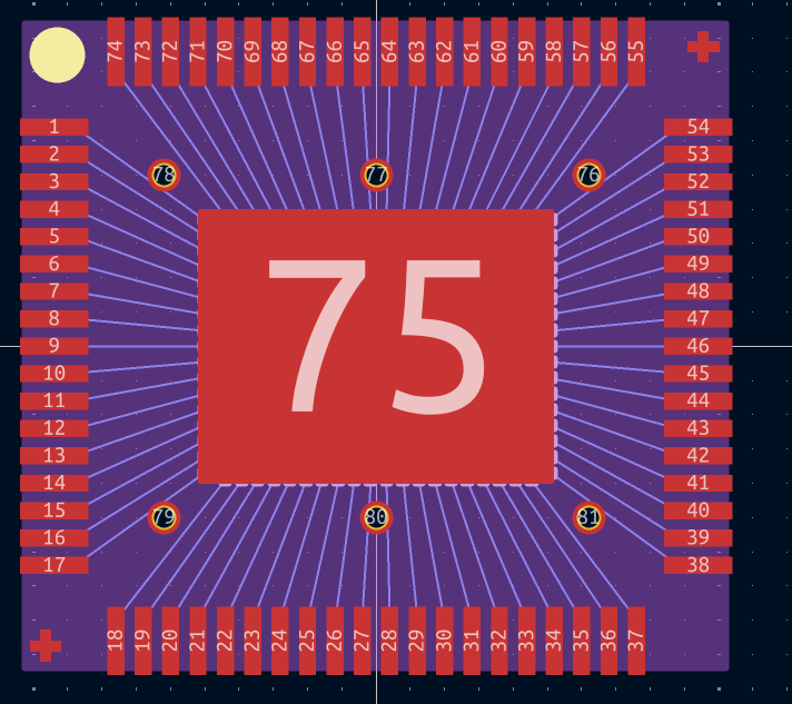
Yes, I should update the picture. The schematic symbol could be more useful.
12:29 p.m.
You can have this one if you like
👍 1
Avatar
This is maybe more in line with what you're thinking. Now things are landscape but the numbering fits convention a little better. Conventions are hard and not everyone will always agree on things. Another one that has thrown me many times using CAD packages is top Americans think of the screen as a window to a virtual world and top is Z+ and does not matter which way you are facing Germans have top as Y+ as if you're imagining the virtual world extending from the tip of your nose. It's hard to say that one is the correct way of doing things.
👍 1
Avatar
ReJ aka Renaldas Zioma 2025-11-23 5:35 p.m.
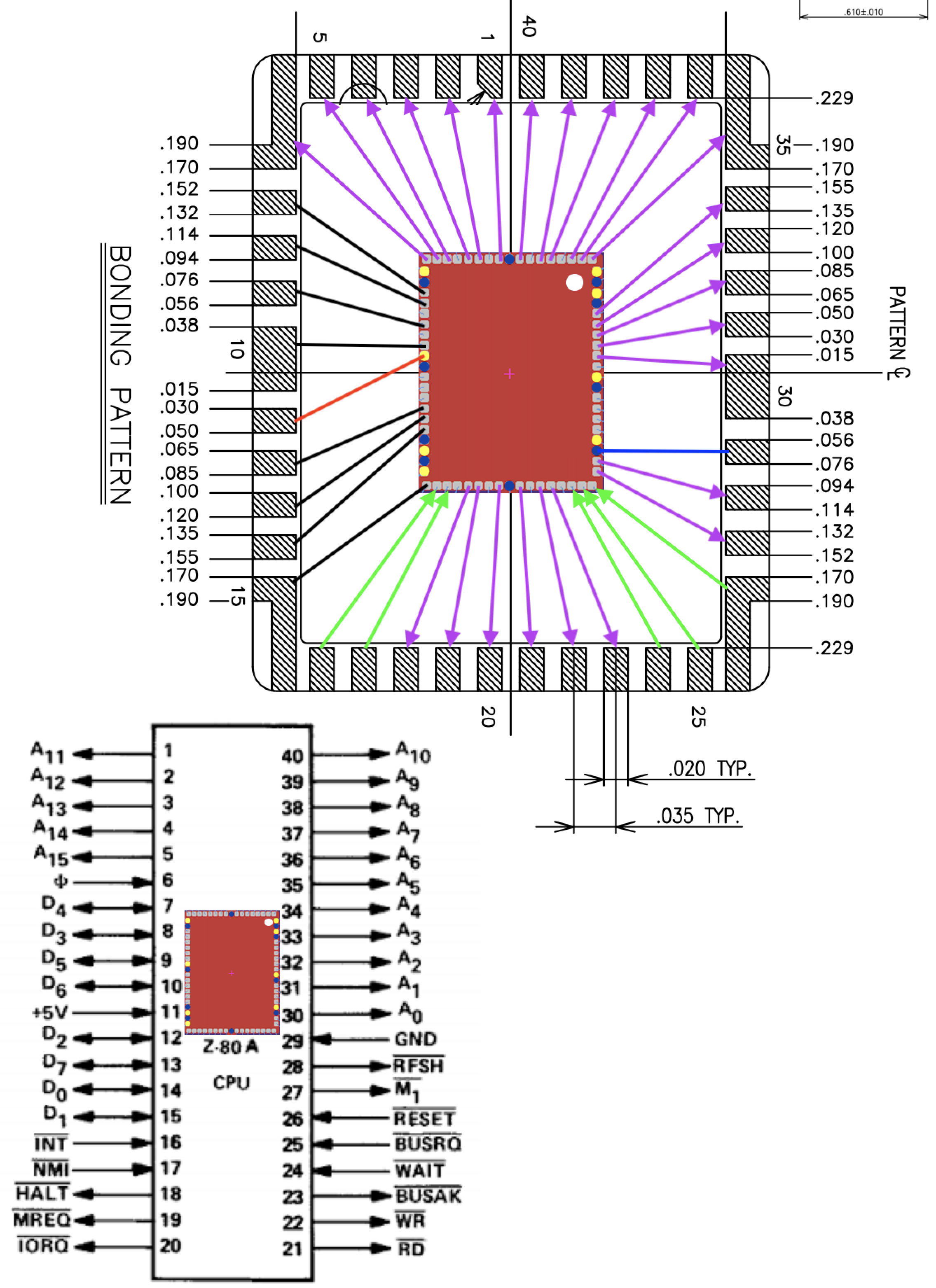
@Tholin FYI, for fun I put chip on top of the diagram for ceramic package that you shared. Although some Z80 wires seems to be problematically bent, maybe it is not too bad. I don't think ceramic package is in the books for this run, but still interesting to entertain the idea. Z80 here has a certain advantage of VDD being on the side of DIP40 (pin 11) rather than 20/40. (edited)
5:35 p.m.
Avatar
I'll give this channel a read over tonight, but I'm curious if anyone could answer this faster. Are there any considerations for wirebonding > 70 pins? My design will be roughly 128 pins. I'm swamped currently with the tapeout finalizing my design, but I would be willing to look into doing a dual 70 pin mezzanine connector OR a larger pin mezzanine connector if that might help after the tapeout.
Avatar
Avatar
Trevor Peyton
I'll give this channel a read over tonight, but I'm curious if anyone could answer this faster. Are there any considerations for wirebonding > 70 pins? My design will be roughly 128 pins. I'm swamped currently with the tapeout finalizing my design, but I would be willing to look into doing a dual 70 pin mezzanine connector OR a larger pin mezzanine connector if that might help after the tapeout.
The standard padframe is 74 pins. You are free to do whatever you like, but going against the standard will likely end up with you having to make your own solutions. There are larger pin versions, but 70 seemed good at that fit the needs of most at the time. There were conversations about using multiple connectors, but there were concerns over tolerances and like I said above, 70pins was adequate.
Avatar
@Andrew Wingate Understood I'll try to find those conversations and read them over.
Avatar
Avatar
Trevor Peyton
@Andrew Wingate Understood I'll try to find those conversations and read them over.
sure, I posted quite a few pictures around those conversations, so searching has: images and maybe from: @Andrew Wingate could help edit also add in: cob as it's in this channel (edited)
👍 1
Avatar
Avatar
Andrew Wingate
sure, I posted quite a few pictures around those conversations, so searching has: images and maybe from: @Andrew Wingate could help edit also add in: cob as it's in this channel (edited)
Man this is so close. My design needs bare minimum 64 parallel pin bus + a clock signal and rst... Everything else I can cut. It looks like there are exactly 64 GPIO pins free which means I'm two short for the design to work! I'll read later and see if I can change some things around my design, I'd like to use the standard wirebond option if I can make it work. Scratch that it looks like a little less I just eyeballed it. (edited)
Avatar
Avatar
Trevor Peyton
Man this is so close. My design needs bare minimum 64 parallel pin bus + a clock signal and rst... Everything else I can cut. It looks like there are exactly 64 GPIO pins free which means I'm two short for the design to work! I'll read later and see if I can change some things around my design, I'd like to use the standard wirebond option if I can make it work. Scratch that it looks like a little less I just eyeballed it. (edited)
There are something like 10 ground pins on the standard cob, it isn't necessary to have the routing down the cob stay the same as the default. The part (for now) that seems most important is to keep the wirebonding pads (qty74) and the 74 pads in the default padring, then also the actual PCB to keep the 14x16mm size and the 70pin mezzanine. @xianglin_pu and the Mosbius team have created their own routing to gain some extra pins by not having so many vss/vcc etc. https://discord.com/channels/1361349522684510449/1429068742108909638/1429520076536811622
Avatar
Avatar
Andrew Wingate
There are something like 10 ground pins on the standard cob, it isn't necessary to have the routing down the cob stay the same as the default. The part (for now) that seems most important is to keep the wirebonding pads (qty74) and the 74 pads in the default padring, then also the actual PCB to keep the 14x16mm size and the 70pin mezzanine. @xianglin_pu and the Mosbius team have created their own routing to gain some extra pins by not having so many vss/vcc etc. https://discord.com/channels/1361349522684510449/1429068742108909638/1429520076536811622
That is perfect! 68 Signal Pins would do it. I'm not framiliar with wirebond process. I'm assuming it's the mapping from the pads to the PCB, are you saying it's possible for us to design our own routing for the PCB and just use the pads as needed?
Avatar
Avatar
Trevor Peyton
That is perfect! 68 Signal Pins would do it. I'm not framiliar with wirebond process. I'm assuming it's the mapping from the pads to the PCB, are you saying it's possible for us to design our own routing for the PCB and just use the pads as needed?
A lot is still unknown, we're trying to keep as much standard as is practical possible, but for now, yes, you can have your own routing on the PCB. Keep in mind that I'll likely be taking another pass and there will be some small changes, so you may want to hold off on designing something now, but overall yes, you can have your own routing on the PCB itself. (edited)
Avatar
Avatar
Andrew Wingate
A lot is still unknown, we're trying to keep as much standard as is practical possible, but for now, yes, you can have your own routing on the PCB. Keep in mind that I'll likely be taking another pass and there will be some small changes, so you may want to hold off on designing something now, but overall yes, you can have your own routing on the PCB itself. (edited)
Sounds good. If the 68 signal pin version is available, I'll just bank on that for now and keep my design. After the tapeout I'll see where everyone is at and go from there, I haven't had time to look at the PCB design yet anyways. I'll give this channel a read later and hopefully be a little more informed. Thanks for the discussion.
👍 1
Avatar
ReJ aka Renaldas Zioma 2025-11-30 1:57 p.m.
@Leo Moser (mole99) FYI, Z80 in quarter size would be almost ceramic package-able, if not for 1 ground that is in the way...
Avatar
Avatar
ReJ aka Renaldas Zioma
@Leo Moser (mole99) FYI, Z80 in quarter size would be almost ceramic package-able, if not for 1 ground that is in the way...
Leo Moser (mole99) 2025-11-30 2:01 p.m.
We might redo the default pinout for the second shuttle, since we may require additional power/ground pads. Perhaps we could find a pinout that works for ceramic as well.
👍 1
Avatar
a ceramic package would be so pretty (edited)
❤️ 1
Exported 103 message(s)
Timezone: UTC+0