Guild icon
wafer.space Community
📐 - Designing / 📦-cob
Channel for discussing chip-on-board packaging options for wafer.space bare die.
Between 2026-04-30 11:59 p.m. and 2026-06-01 12:00 a.m.

Avatar
Avatar
RebelMike
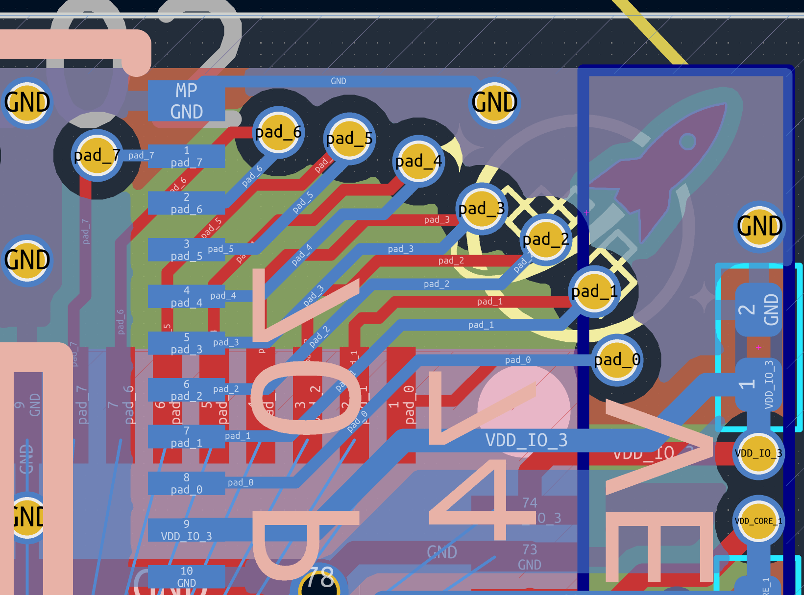
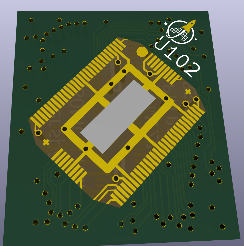
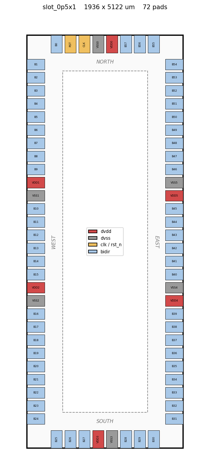
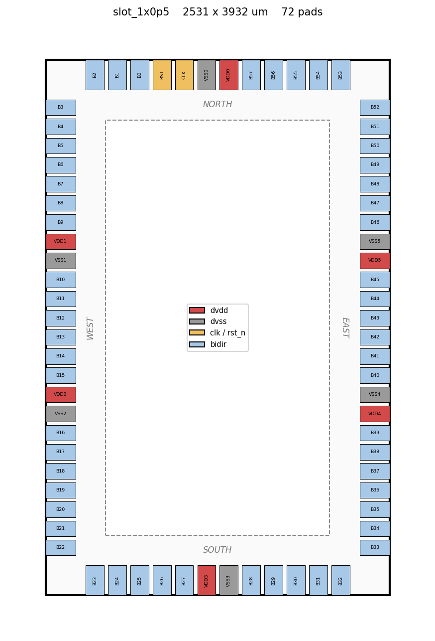
Finished routing the 1x0p5 version. Pinout of power, clk, rst_n and bidirs matches 1x1. I suspect matching the 0p5x1 will be rather tricky. Quarter size should be easier as the pad frame will be smaller giving a bit more space for routing.
Tim 'mithro' Ansell 2026-05-01 1:55 a.m.
Great work Mike!
Avatar
Avatar
namibj
Also, not sure how the bonding palce likes it, but if you need routing access, do consider rotating 45 degrees.
Tim 'mithro' Ansell 2026-05-01 1:55 a.m.
From what I have seen so far, I don't think the bond house we are using will care at all.
1:59 a.m.
@RebelMike / @Greg - It is very likely whatever we end up using on the TinyQV and/or Racquet die will become the standard CoB layout for the non-1x1 projects getting packaged.
2:01 a.m.
@RebelMike / @Greg / @Leo Moser (mole99) - I'm also open to the alternative idea of changing the GF180MCU template I/O allocations for these sizes to make things easier.
Avatar
Brian Swetland 2026-05-01 2:05 a.m.
a pin 1 marker on the silkscreen for the mezzanine connector might be nice just for completeness
Avatar
Avatar
Brian Swetland
a pin 1 marker on the silkscreen for the mezzanine connector might be nice just for completeness
Might wrongly suggest polarization.
Avatar
just got my motherboard breakout PCBs ... i severely underestimated how small the connector pins/pads would be 😅 probably should have bought a stencil to go with it, guess we'll see how good I am at fine soldering!
💜 1
Avatar
Avatar
BreakingTaps
just got my motherboard breakout PCBs ... i severely underestimated how small the connector pins/pads would be 😅 probably should have bought a stencil to go with it, guess we'll see how good I am at fine soldering!
Tim 'mithro' Ansell 2026-05-01 2:30 a.m.
Hot Air reflow and a good (pre-)heating plate helps a lot, surface tension is your friend.
👍 1
Avatar
Avatar
RebelMike
I don't actually see the new padring in your branch - maybe forgot to add the file?
Andrew Wingate 2026-05-01 3:36 a.m.
Sorry, it seems I didn't hit save before I hit commit.
Avatar
Avatar
Tim 'mithro' Ansell
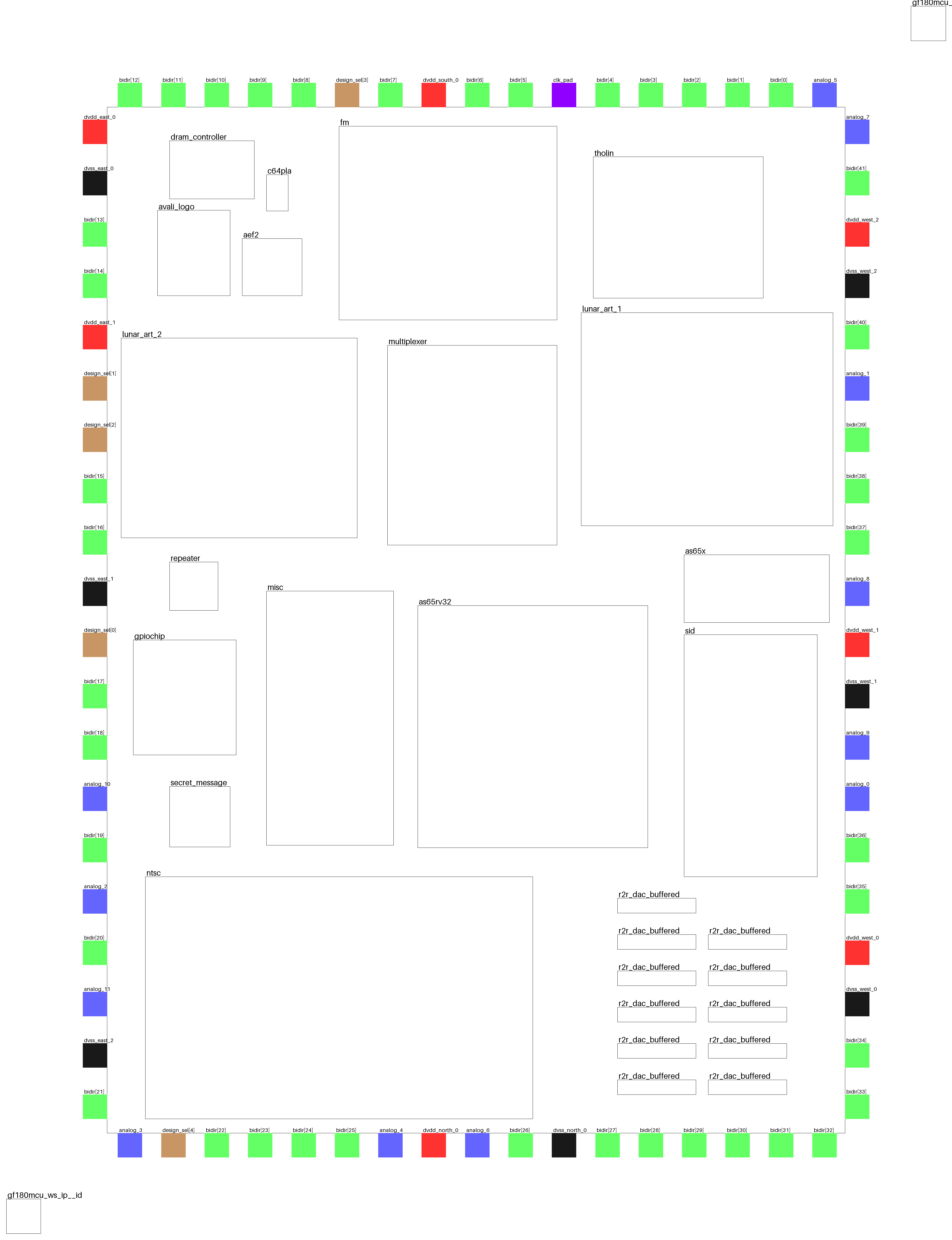
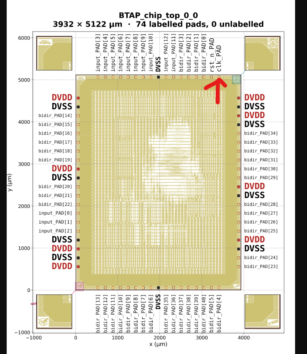
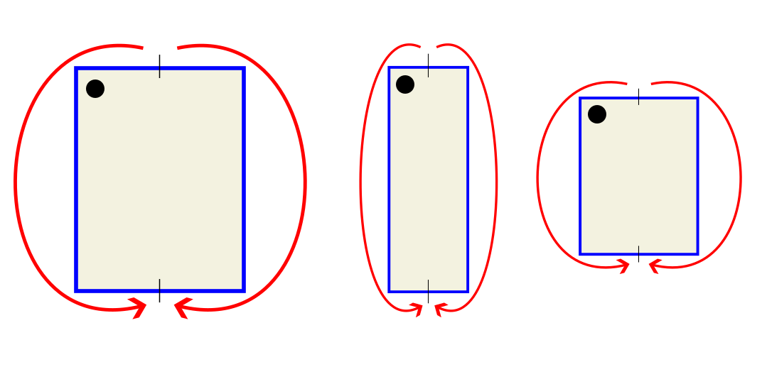
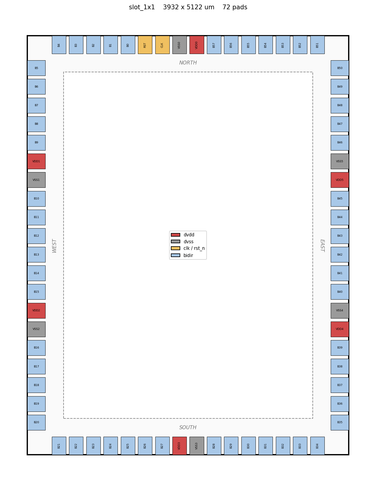
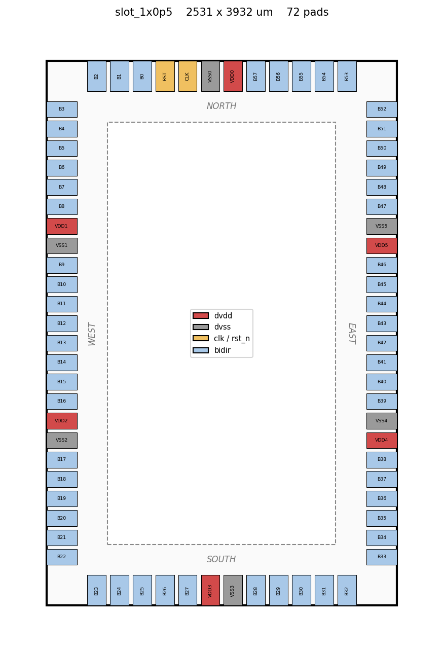
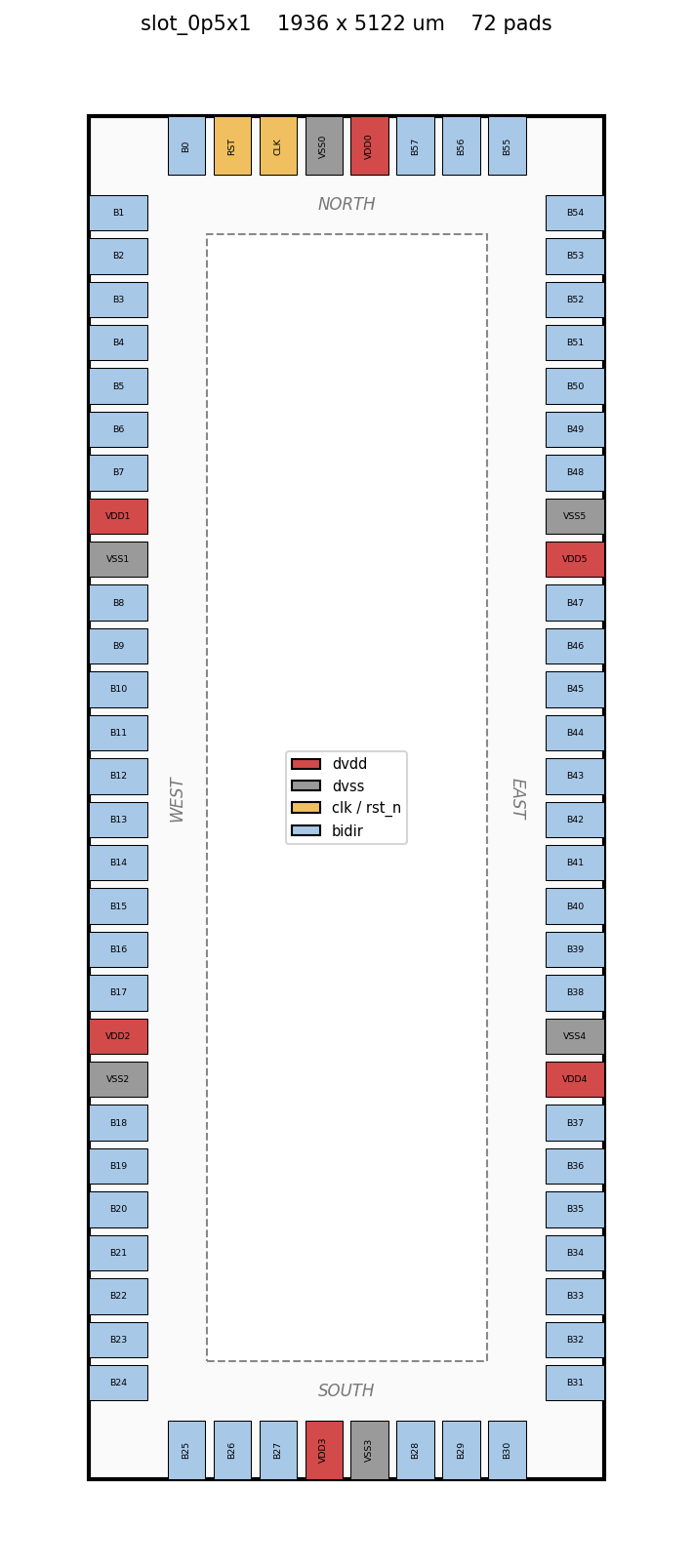
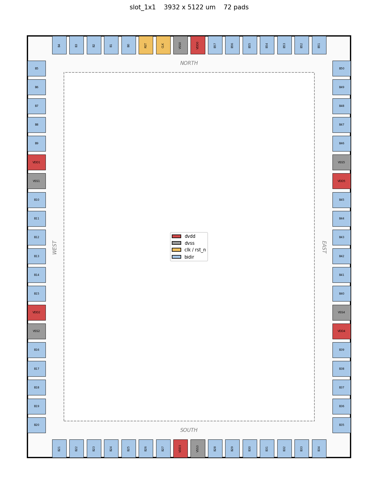
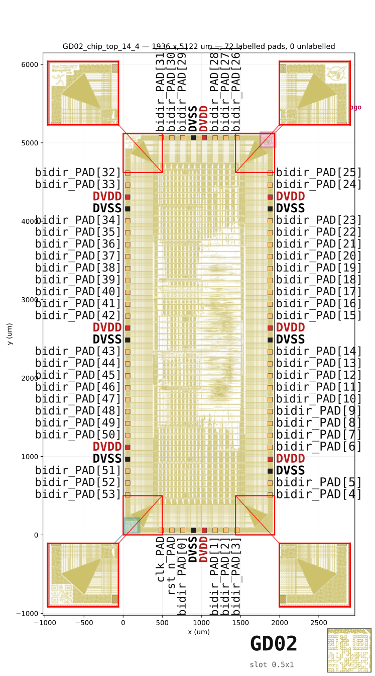
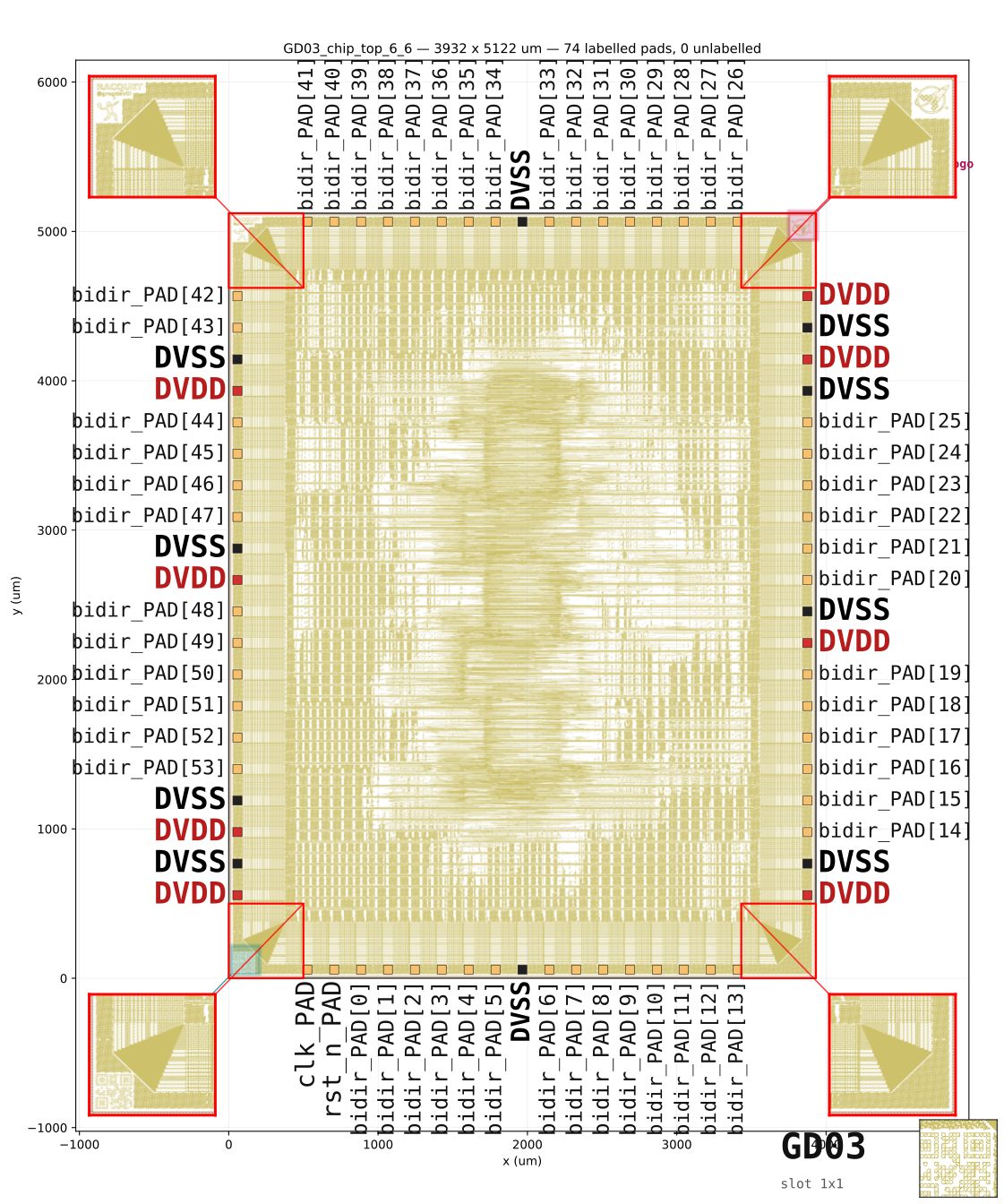
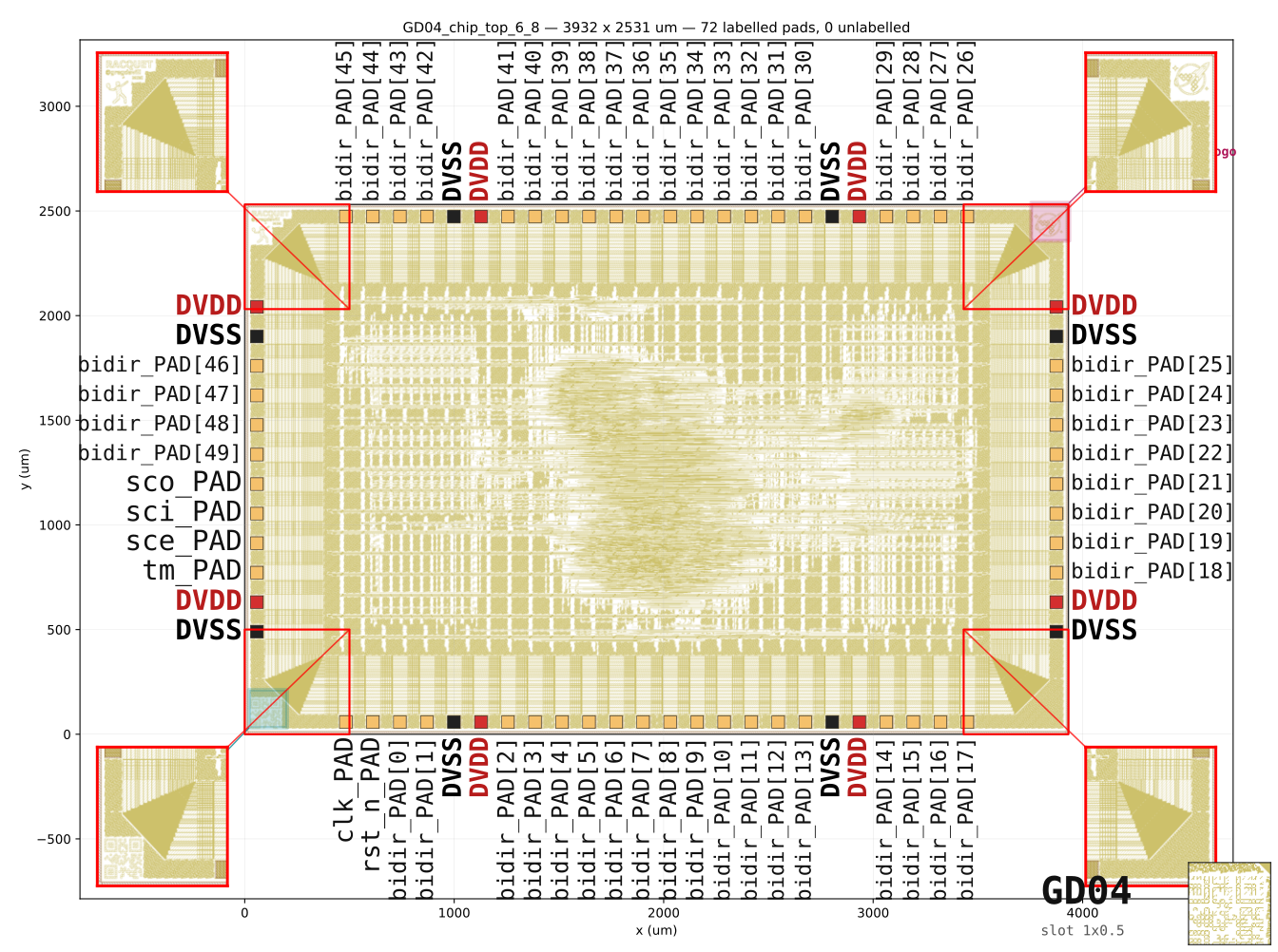
These are the three diagrams I generated for @Greg chips.
Do you have the scripts which generated this? Would be nice to get an SVG if possible to put into the datasheet/spec for the chip
Avatar
Avatar
RebelMike
Finished routing the 1x0p5 version. Pinout of power, clk, rst_n and bidirs matches 1x1. I suspect matching the 0p5x1 will be rather tricky. Quarter size should be easier as the pad frame will be smaller giving a bit more space for routing.
Was this checked in somewhere? I'm happy to take a look and poke around with the bonding for the 0p5x1
Avatar
Avatar
Greg
Was this checked in somewhere? I'm happy to take a look and poke around with the bonding for the 0p5x1
Wire bonded chip on board PCB designs. Contribute to MichaelBell/chip-on-board-wire-bonded-pcbs development by creating an account on GitHub.
👍 1
Avatar
Avatar
Greg
Do you have the scripts which generated this? Would be nice to get an SVG if possible to put into the datasheet/spec for the chip
Andrew Wingate 2026-05-01 6:49 a.m.
I am told these may be partially out of date, but here you go!
Avatar
Avatar
Greg
Was this checked in somewhere? I'm happy to take a look and poke around with the bonding for the 0p5x1
Ah, no it isn't - apparently I was on Andrew's branch and committed and pushed it there. I'll merge that
Avatar
I'll also make a PR against the main repo. But possibly after I've had some coffee 🙂
Avatar
No worries, I'll only get to looking at this in depth in a few hours
Avatar
Avatar
Greg
Do you have the scripts which generated this? Would be nice to get an SVG if possible to put into the datasheet/spec for the chip
Tim 'mithro' Ansell 2026-05-01 7:02 a.m.
It is a super horrific AI written bit of code. Let me see if I can upload it somewhere. At some point I think I'm (or really I'm going to have a better attempt at AI doing it) going to try and write/good a proper version and integrate it into either https://platform.wafer.space or maybe even LibreLane.
Platform for wafer.space low cost silicon manufacturing.
💜 1
7:03 a.m.
@Leo Moser (mole99) / @Andrew Wingate - I just had the thought that maybe it should be LibreLane that is generating Andrew's KiCAD footprints + wire bonding diagrams and my random pin out diagrams?
Avatar
Avatar
Tim 'mithro' Ansell
@Leo Moser (mole99) / @Andrew Wingate - I just had the thought that maybe it should be LibreLane that is generating Andrew's KiCAD footprints + wire bonding diagrams and my random pin out diagrams?
Tim 'mithro' Ansell 2026-05-01 7:03 a.m.
@Leo Moser (mole99) - Terrible or good idea? 😛
Avatar
Avatar
Tim 'mithro' Ansell
@Leo Moser (mole99) / @Andrew Wingate - I just had the thought that maybe it should be LibreLane that is generating Andrew's KiCAD footprints + wire bonding diagrams and my random pin out diagrams?
Andrew Wingate 2026-05-01 7:04 a.m.
I don't know how that would work? You must specify a standard wirebonding frame first? Like from a set?
Avatar
Not sure if Librelane, but a script that could generate the correct sized pad + drawing annotations in the exact pin positions could be useful. For the whole padring I guess it would be possible at least for a standard rectangular one - just push the pins out until the 45 degree rule wasn’t violated
Avatar
Avatar
Tim 'mithro' Ansell
@RebelMike / @Greg / @Leo Moser (mole99) - I'm also open to the alternative idea of changing the GF180MCU template I/O allocations for these sizes to make things easier.
Yeah I don’t know how much thought was given to the pin allocations for the different sizes - I suspect @Leo Moser (mole99) was just trying things out. Potentially we try to route them all to match the existing template as much as possible, then change the template to make them match completely? Though I suspect in general this doesn’t matter too much - the case of wanting them to match has only really come up because TinyQV was used in different slot sizes as a test.
Avatar
Avatar
RebelMike
Yeah I don’t know how much thought was given to the pin allocations for the different sizes - I suspect @Leo Moser (mole99) was just trying things out. Potentially we try to route them all to match the existing template as much as possible, then change the template to make them match completely? Though I suspect in general this doesn’t matter too much - the case of wanting them to match has only really come up because TinyQV was used in different slot sizes as a test.
Tim 'mithro' Ansell 2026-05-01 7:38 a.m.
I think having a "standard" which means people can share "motherboards" PCBs is helpful rather than everyone having to design new ones. (edited)
Avatar
I don’t think a standard mapping of the template pinout is required for that - it’s probably the other way around: if there was a standard SoC host motherboard (with flash, ram, etc) and the pinout for that and all the breakouts was known, you could just wire things up correctly in the silicon.
7:43 a.m.
But I guess that is basically the same as saying make the template match whatever we end up with
Avatar
Avatar
RebelMike
I don’t think a standard mapping of the template pinout is required for that - it’s probably the other way around: if there was a standard SoC host motherboard (with flash, ram, etc) and the pinout for that and all the breakouts was known, you could just wire things up correctly in the silicon.
Andrew Wingate 2026-05-01 7:50 a.m.
That is a good point though to think about some things upstream instead of all downstream. Thanks for the thought
Avatar
Tim 'mithro' Ansell 2026-05-01 12:38 p.m.
@Greg - Don't say I didn't warn you 😛 - https://github.com/mithro/wafer-space-die-pad-diagrams
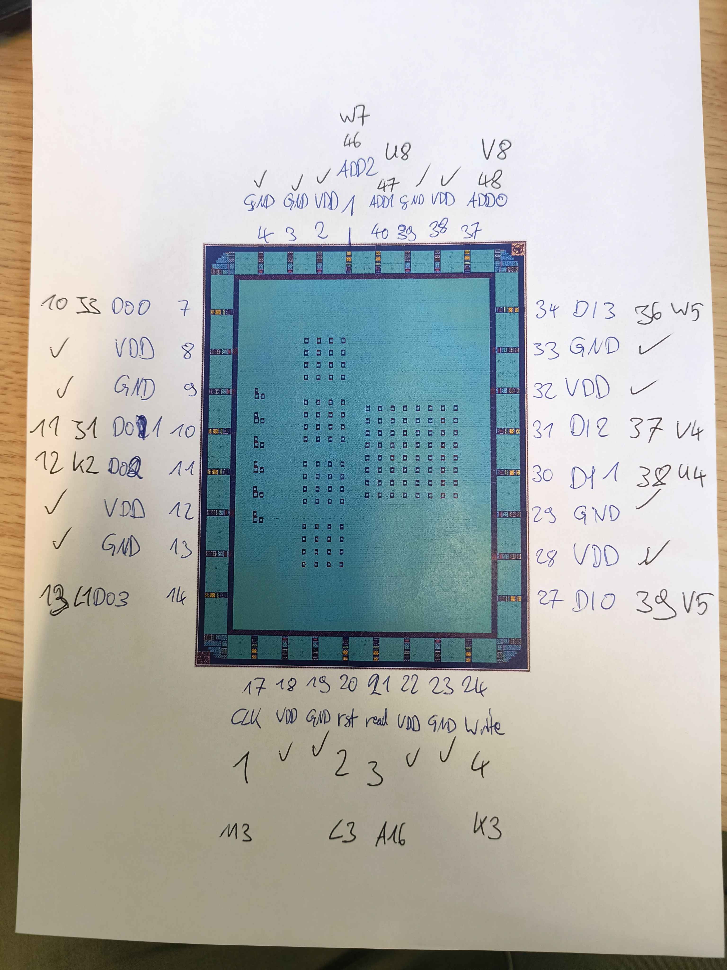
Contribute to mithro/wafer-space-die-pad-diagrams development by creating an account on GitHub.
❤️ 1
Avatar
Avatar
Tim 'mithro' Ansell
@Greg - Don't say I didn't warn you 😛 - https://github.com/mithro/wafer-space-die-pad-diagrams

That looks much more professional than what I did 😅
1:43 p.m.
Avatar
Andrew Wingate 2026-05-01 2:26 p.m.
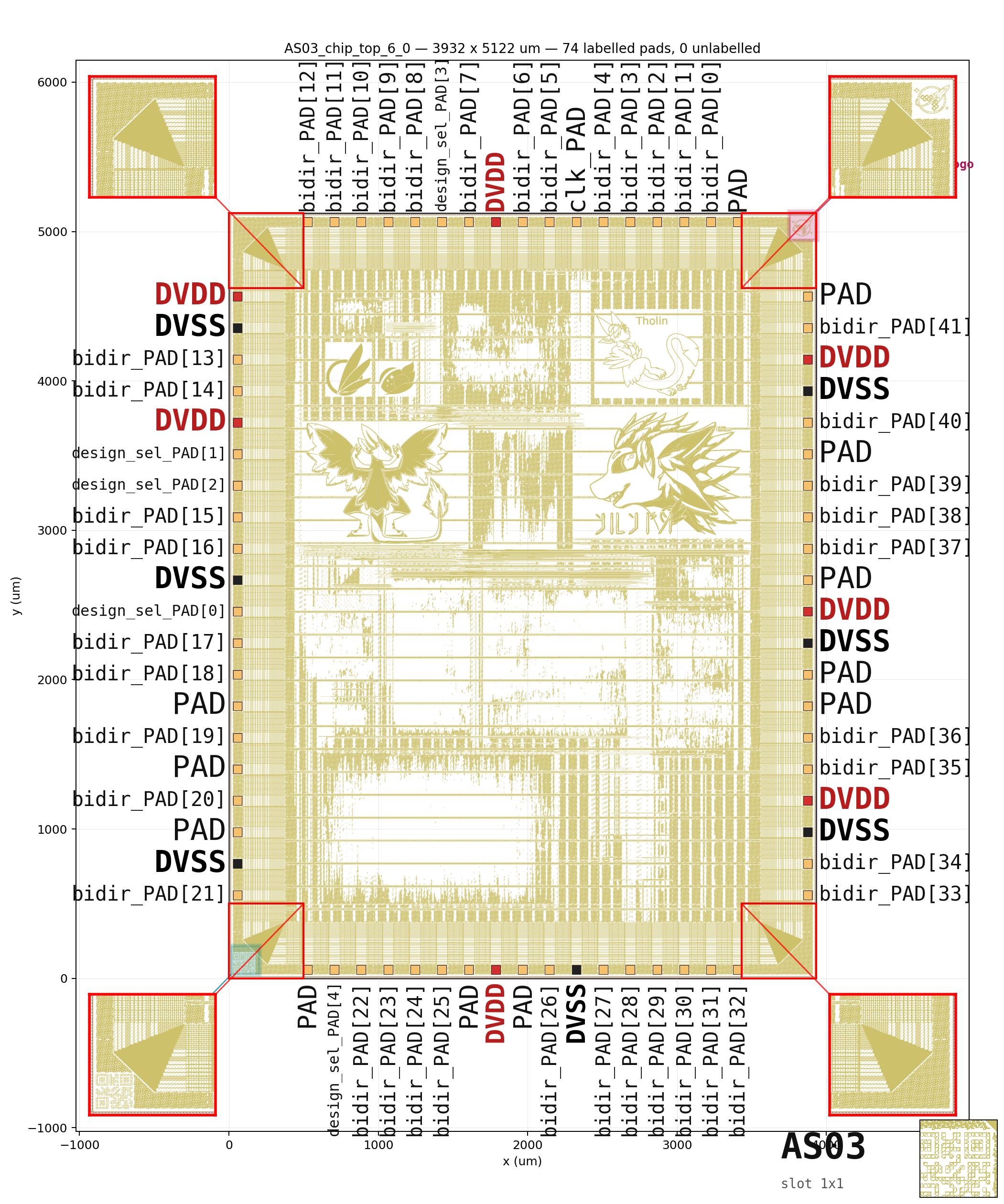
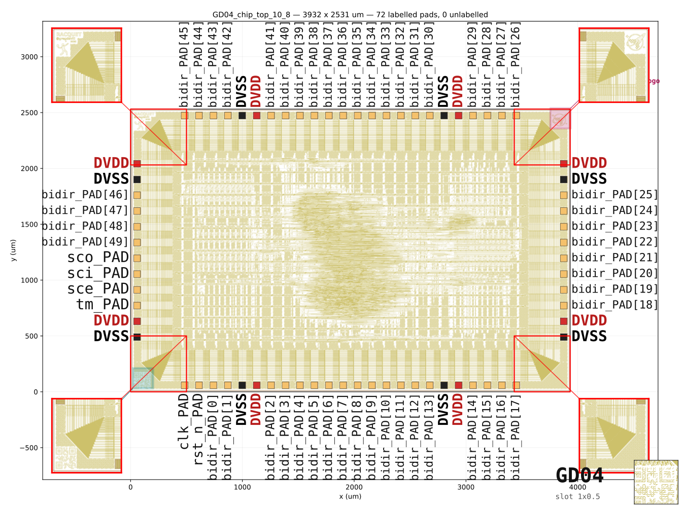
@Tholin here's yours, anyone else can have theirs if they wish. We're looking to integrate this into the verification system, so you'd just get one anyways.
2:27 p.m.
Yours is still very neat that is shows the sub-projects as well!
Avatar
To show the macro locations is a bit tricky. The position of each macro is specified in the librelane config, but to get its size, you need to open up its LEF.
👍 1
Avatar
Avatar
Andrew Wingate
@Tholin here's yours, anyone else can have theirs if they wish. We're looking to integrate this into the verification system, so you'd just get one anyways.
I see the analog pads are all just labeled "PAD" in this
Avatar
Avatar
Tholin
I see the analog pads are all just labeled "PAD" in this
Andrew Wingate 2026-05-01 2:35 p.m.
Yeah, we were talking earlier about pincounts and what's actually needed. How many of the pins did you end up using for real? all of them? Most of them?
Avatar
All of them
💯 1
Avatar
Avatar
Tholin
All of them
Andrew Wingate 2026-05-01 2:41 p.m.
Like I said we were talking about some reduced pin counts. In your opinion what's a reasonable low number?
2:41 p.m.
*lower
Avatar
I always need as many as possible for my processor designs for memory throughput
🤣 1
2:43 p.m.
I can finally build 32-bit wide data buses on wafer.space
Avatar
Andrew Wingate 2026-05-01 2:43 p.m.
It's all good. There really is no answer. Ah, ok, that's a good thought.
Avatar
My GFMPW-1 RISC-V core multiplexes both halves of the address and both halves of a word onto the same 16 pins
2:43 p.m.
4 clock cycles for a single instruction fetch, worst case (edited)
2:44 p.m.
3 clock cycles best case
Avatar
Andrew Wingate 2026-05-01 2:44 p.m.
I see. Thanks for the insight
Avatar
wafer.space still doesn’t give enough pins for separate address and data buses on a 32-bit CPU without compromises, but its almost there
👍 1
Avatar
Andrew Wingate 2026-05-01 2:46 p.m.
Getcha, the question revolved around trying to come up with some less expensive cob or packaging alternatives.
Avatar
CHES uses 4 GPIOs for JTAG and 11 for ULPI
💜 1
3:00 p.m.
(if that's a useful datapoint)
Avatar
Avatar
Lofty
(if that's a useful datapoint)
Andrew Wingate 2026-05-01 3:01 p.m.
They are all useful. Thank you. I think we just need to put together some numbers and see where any kind of step functions are.
Avatar
(side note, I don't suppose there's a way to manually annotate the pad diagrams with actual pin functions rather than the toplevel pin name)
Avatar
Unfortunately, we are talking about integrated circuits, where IO is often the bottleneck
Avatar
Andrew Wingate 2026-05-01 3:08 p.m.
Does this data exist somewhere? If it exists and people will use it we can incorporate it into the pipeline
Avatar
Avatar
Tholin
Unfortunately, we are talking about integrated circuits, where IO is often the bottleneck
ULPI was my solution to that problem :p
Avatar
Avatar
Andrew Wingate
Does this data exist somewhere? If it exists and people will use it we can incorporate it into the pipeline
uh, I have it as source code defines; nothing more structured if that's what you're asking for
Avatar
Andrew Wingate 2026-05-01 3:09 p.m.
Can you share what that acronym is?
Avatar
Avatar
Lofty
uh, I have it as source code defines; nothing more structured if that's what you're asking for
Andrew Wingate 2026-05-01 3:09 p.m.
I see, if there's a way to get it into the GDS that's our source of truth.
Avatar
Avatar
Andrew Wingate
Can you share what that acronym is?
UTMI+ Low Pin Interface; uh, USB Hi Speed PHY interface
💜 1
3:10 p.m.
which means I can do 480Mbps serial (well, theoretically) while having my chip only have to achieve 60MHz
Avatar
I mean, particularly for memory. Ever CPU I ever taped out on gf180mcu was memory bottlenecked. Caravel was aggressively memory bottlenecked.
Avatar
Andrew Wingate 2026-05-01 3:11 p.m.
I know Tim has been interested in SerDes, this can probably help with pincounts someday as well?
👍 1
🎉 1
Avatar
Avatar
Tholin
I mean, particularly for memory. Ever CPU I ever taped out on gf180mcu was memory bottlenecked. Caravel was aggressively memory bottlenecked.
Andrew Wingate 2026-05-01 3:11 p.m.
I am marginally aware how they didn't let you do a lot
Avatar
(although I feel like at that point we need a better standard cell library >.>)
💯 1
3:12 p.m.
(this is not directed at Tholin, it's directed at myself to try to get back to working on my synthesisable domino logic library)
waferspace 1
Avatar
There is a lot I need to improve about my SCL before I’m fully confident in it
Avatar
It also doesn't help that I'm having to work with custom timing extraction scripts from ngspice to characterise the cells
3:23 p.m.
I also think my library will probably have to rely on yours for the non-logic stuff because I have zero clue what to do there
Avatar
Avatar
Andrew Wingate
Getcha, the question revolved around trying to come up with some less expensive cob or packaging alternatives.
Tiny Tapeout offers 26 pins (plus any analog pins) so 26-30 might be something to consider for a lower cost option on the smaller slots. Although Wafer Space is quite a different offering to TT people might prototype on TT and then bring things across. It might also be interesting to have a higher pin count option for the full size slot.
💯 1
Avatar
Andrew Wingate 2026-05-01 3:45 p.m.
I don't think there are any plans to lower any counts, only to try to offer a lower cost version.
Avatar
I guess I was thinking it might be interesting to have the current option (56 IOs) plus a smaller option (~26 IOs) for the half slots. And the current option plus a larger option (~80 IOs?) on the full slot.
3:52 p.m.
Though the larger option would obviously need a different connector (presumably 2x50) - I know there was some concern about two connectors but TT should soon find out if that causes any problems
Avatar
Andrew Wingate 2026-05-01 3:54 p.m.
2x mezzanine was shunned pretty hard by those here, so I don't see that as an option. Maybe if we can get back to looking at some kind of LGA or something. https://discord.com/channels/1361349522684510449/1408134567491145728/1426376335709966446
Avatar
Yeah I remember that discussion but I think it was probably over cautious. But the new TT boards should be a good indicator of whether it’s a problem in practice (they have 2x mezzanine)
👍 1
Avatar
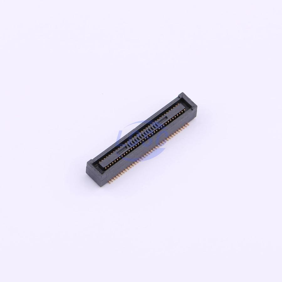
I was going to use this for my daughter/motherboard cards: HC-PBB40C-90DP-0.4V-02 it's a 90 pin version, much easier than a 2x50 (in my opinion). (edited)
4:05 p.m.
HC-PBB40C-90DP-0.4V-02 from HCTL - Board-to-Board and Backplane Connector is available for JLCPCB assembly, check the stock, pricing and datasheet, and let JLCPCB helps you assemble the part HC-PBB40C-90DP-0.4V-02 for free.
👍 1
👀 1
Avatar
Avatar
Tholin
wafer.space still doesn’t give enough pins for separate address and data buses on a 32-bit CPU without compromises, but its almost there
DDR to the rescue?
Avatar
Tim 'mithro' Ansell 2026-05-02 2:31 a.m.
Contribute to mithro/wafer-space-die-pad-diagrams development by creating an account on GitHub.
Avatar
Avatar
Lofty
CHES uses 4 GPIOs for JTAG and 11 for ULPI
Tim 'mithro' Ansell 2026-05-02 2:33 a.m.
You have a ULPI USB interface?
2:36 a.m.
At the current time packaging is a large part of the cost here and packaging is driven up by the number of IO pins. IO pads also take up quite a bit of die space. Hence figuring out options for SERDES and other ways to reduce pin count is something I'm very interested in.
Avatar
Avatar
Tim 'mithro' Ansell
You have a ULPI USB interface?
Yes
Avatar
Tim 'mithro' Ansell 2026-05-02 6:24 a.m.
@Lofty - Cool! I think having a bunch of proven USB connectivity solutions would be a huge gain for community.
6:24 a.m.
@tnt also had some type of USB interface on the Tiny Tapeout chip.
Avatar
Avatar
Tim 'mithro' Ansell
@Lofty - Cool! I think having a bunch of proven USB connectivity solutions would be a huge gain for community.
I knew I was going to be bandwidth hungry but also needed some kind of standard communication interface; at one point the plan was to have the chip be its own PHY and run at Full Speed, but then it was suggested that I could use ULPI and aim for Hi Speed instead.
Avatar
Tim 'mithro' Ansell 2026-05-02 6:29 a.m.
FWIW - The original design doc for Caravel had it providing a high speed interface between your tape out and a computer and a whole bunch of "virtual" digital and analog pins that could be queried via virtual logic analyser / virtual oscilliscope so the limited number of pins that we could provide cost effectively was less of an impact, but that never quite happened.
6:30 a.m.
I'm still interested in reaching that type of goal.
Avatar
Avatar
Tim 'mithro' Ansell
At the current time packaging is a large part of the cost here and packaging is driven up by the number of IO pins. IO pads also take up quite a bit of die space. Hence figuring out options for SERDES and other ways to reduce pin count is something I'm very interested in.
If you have a little space (it's the smallest analog tile on ttsky26a, but you'd probably want higher current output drivers if they don't have to go through an analog mux), two analog pads, and some tt-style Mux'd digital access, and would give a functioning one to @azonenberg for characterization, I'd put considerable effort into porting my currently-in-progress ttsky26a submission to gf180mcud in time for the wafer.space Run2 GDS deadline. (I hope to assume correctly that there is deep-nwell and the capability for placing nmos_03v3_nvt devices with raised bulk in said deep-nwell. And decent models of those in the region just around/above the (effective) threshold. With those "requirements" I'd see no reason why my ttsky26a submission wouldn't be readily portable to Run2. At least for short channels (no backplane or multi-meter Twinax!) an RX design might be possible to attempt before the Run2 deadline.) I'll try my best to get a parasitics-extraction simulation of the VCO core done today so we'd know where things stand both with the VCO itself as well as with an SDR latch fast enough to do a DIV2 on the VCO. No inductors involved. (edited)

Avatar
So has anyone tested their COB package yet ?
Avatar
I will on tuesday
6:49 p.m.
Or... wednesday? The package got delayed?
6:49 p.m.
That’s not good, I’m not home wednesday
6:50 p.m.
Did the COBs get shipped in an envelope (like the dies) or package?
Avatar
Avatar
Tholin
Did the COBs get shipped in an envelope (like the dies) or package?
envelope
Avatar
Oh, very good. Lets hope it fits in my mailbox.
👍 1
Avatar
Avatar
Tholin
Oh, very good. Lets hope it fits in my mailbox.
making you have a mailbox that will fit them (if you ask nicely enough you can probably get fairly good dimensins) could allow you to reduce the need for hope/luck. (I should get me a mailbox that can fit German Maxibrief; C4 (or B4?) at the 3?5?cm thickness, or at least letters of full size (non-folded) without substantial bending....)
Avatar
The envelope with the dies fit
9:38 p.m.
So should be fine
Avatar
Avatar
Tholin
The envelope with the dies fit
(I say this because the COBs are from what I could see at breaking tap's post, slabs of PCB as they were processed at the bond house, not individualized or like the dies, taped.)
Avatar
Andrew Wingate 2026-05-03 3:26 a.m.
@Tim 'mithro' Ansell do we know the formfactor the COB were send in? Envelope or box?
Avatar
Tim 'mithro' Ansell 2026-05-03 3:45 a.m.
@Andrew Wingate - Smaller padded envelope inside a non-padded fedex envelope.
💯 2
Avatar
Tim 'mithro' Ansell 2026-05-03 5:18 a.m.
@Andrew Wingate - BTW Did you share the bond diagrams you are generating here?
Avatar
Avatar
Tim 'mithro' Ansell
@Andrew Wingate - BTW Did you share the bond diagrams you are generating here?
Andrew Wingate 2026-05-03 5:39 a.m.
I only shared Breaking Taps' version. https://discord.com/channels/1361349522684510449/1408134567491145728/1499326875657306113 I can share more if you like.
Avatar
@Greg Does the arrow sticker on the picture mean you found an issue with that particular chip ? (edited)
Avatar
Avatar
stuart
Click to see attachment 🖼️
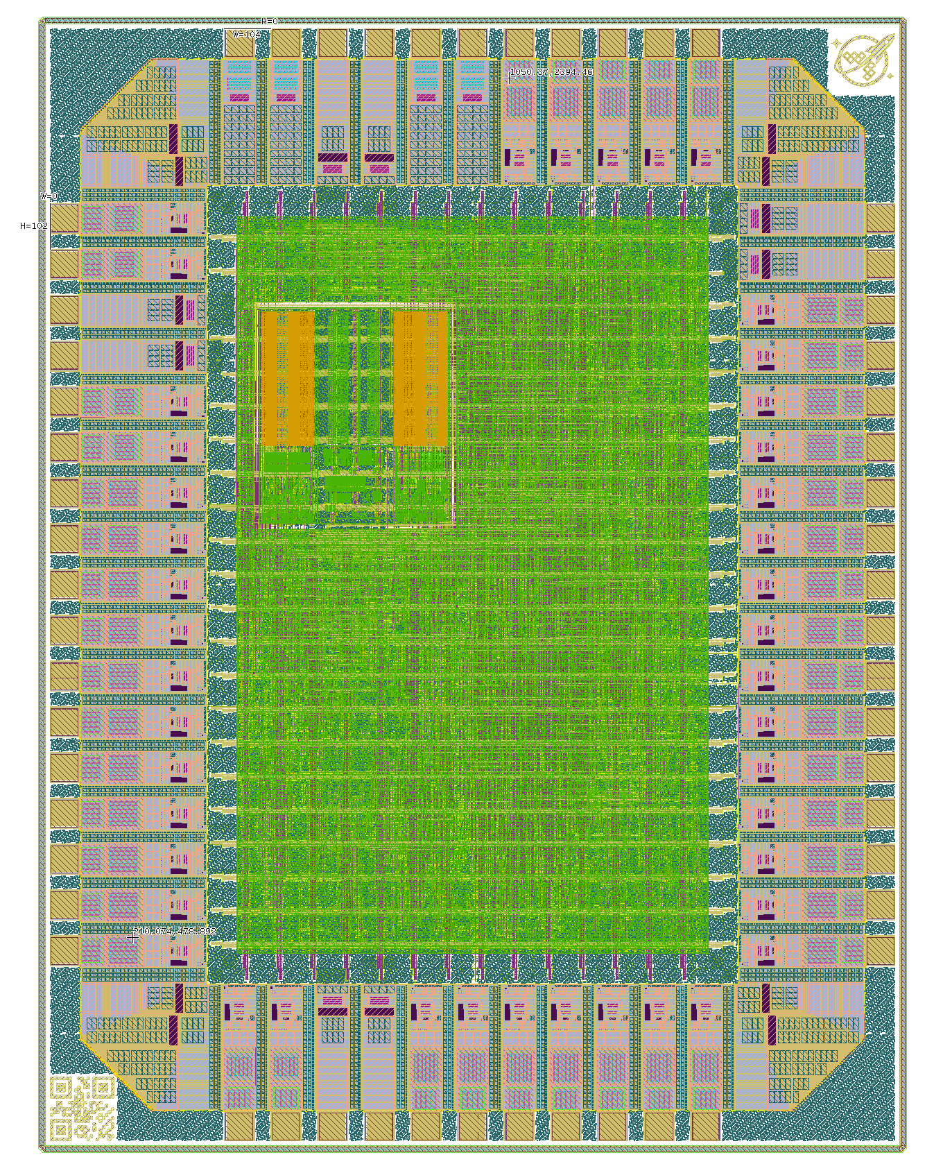
I don’t know how I failed to notice that my dies are upside-down when I looked closely at this. Confirmation bias, probably.
Avatar
I'm looking at https://discord.com/channels/1361349522684510449/1408134567491145728/1495357823314563143 and the pad 0 indicator (which is the one where QR code is on the dies) is on the side of the silk Uxx markers.
3:45 p.m.
Ah yeah, I see. In the repo for the COB PCB the board orientation is not the same as the GDS orientation. https://github.com/wafer-space/chip-on-board-wire-bonded-pcbs/blob/main/74pad-70pin-mezzanine/wirebonding/wirebonding.png
Avatar
I simply expected the top of the GDSII layout to be aligned with the top of the PCB layout, and was never informed otherwise Even in that wireponding.png view, you have to squint to see where the QR Code and logo are.
Avatar
Meinhard Kissich 2026-05-06 4:22 p.m.
How are Vcore, VIO, and Vaux currently/in future used? The cob module routes them separately but they seem to be low-ohmically connected. (edited)
Avatar
Avatar
Meinhard Kissich
How are Vcore, VIO, and Vaux currently/in future used? The cob module routes them separately but they seem to be low-ohmically connected. (edited)
Leo Moser (mole99) 2026-05-06 4:46 p.m.
In the (very) near future, you will be able to have separate voltage domains in your chip by using the wafer.space template. The foundry-provided pads short the core and I/O domain on purpose. This will be possible thanks to Tim's 3.3/5V I/O cells, which have a level shifter between core and I/O domain and keep both domains properly separated in the power/ground pads. As for Vaux, the idea is to provide another voltage domain directly to the core.
👍 1
😮 1
Avatar
Avatar
Leo Moser (mole99)
In the (very) near future, you will be able to have separate voltage domains in your chip by using the wafer.space template. The foundry-provided pads short the core and I/O domain on purpose. This will be possible thanks to Tim's 3.3/5V I/O cells, which have a level shifter between core and I/O domain and keep both domains properly separated in the power/ground pads. As for Vaux, the idea is to provide another voltage domain directly to the core.
Meinhard Kissich 2026-05-06 6:33 p.m.
Great, thanks for the info @Leo Moser (mole99)
👍 1
Avatar
Avatar
tnt
@Greg Does the arrow sticker on the picture mean you found an issue with that particular chip ? (edited)
Yes. that particular one has a lifted bondwire. Found just with a visual inspection. Threw a QC flag so I didn't forget about it.
Avatar
Interesting. I couldn't really tell from the image.
Avatar
Tim 'mithro' Ansell 2026-05-10 2:22 a.m.
@tnt - FWIW @Lauri has been contracted to do an automated tester base around the reverse biasing the ESD diodes like you suggested.
Avatar
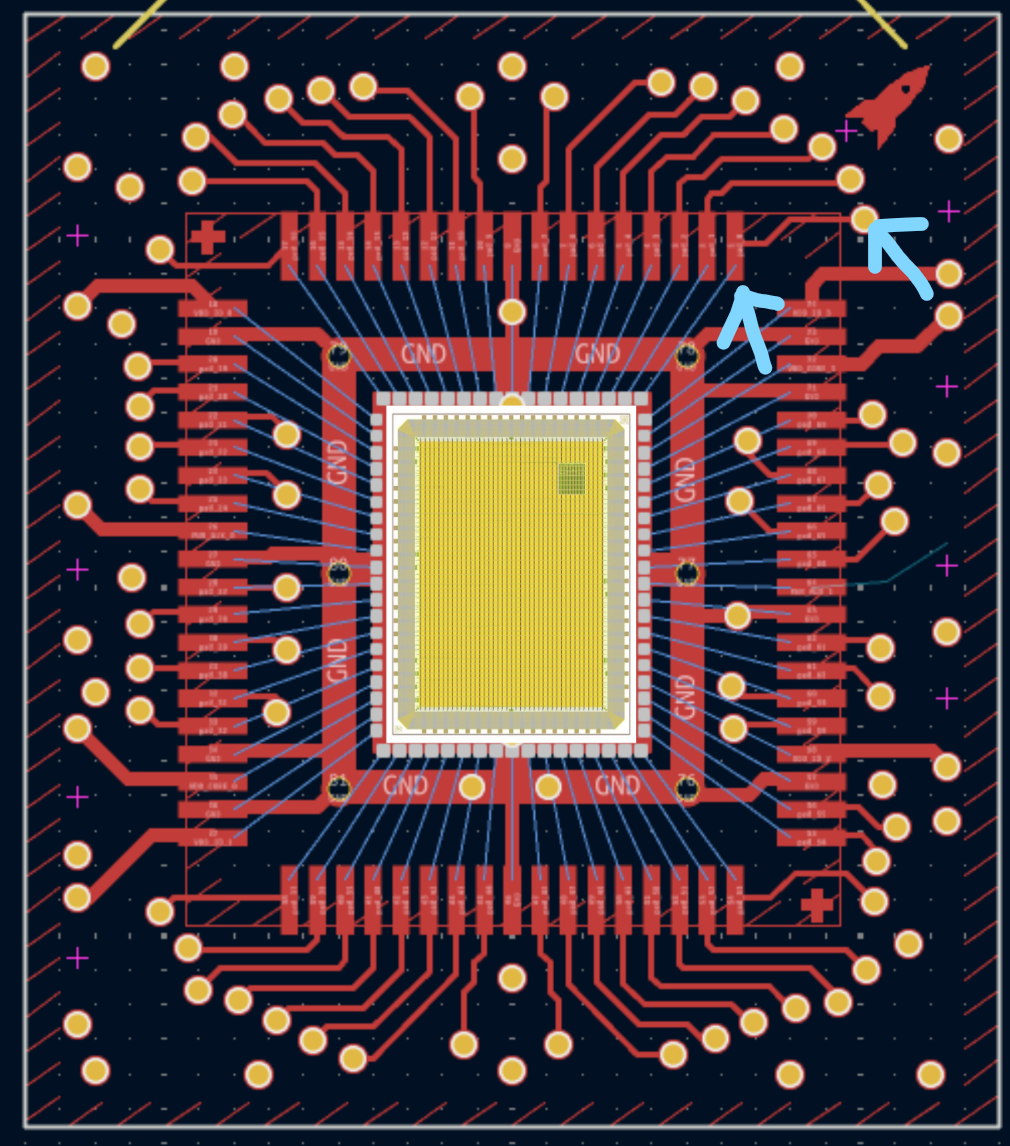
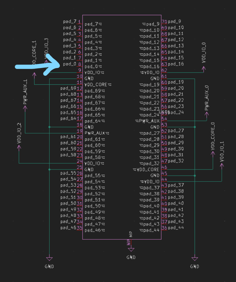
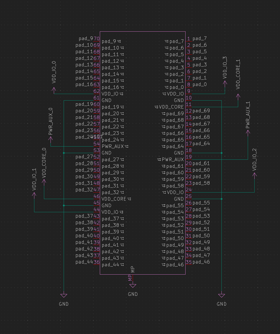
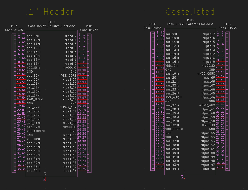
@Andrew Wingate question about the mezzanine breakout board. I'm looking at the die and COB pinout, Pad0 is top right on the die (by QR code) and bonds to top-right pad on COB (by wafer.space logo). So I'm assuming it drops down a via and goes to the right side of the mezzanine connector (while still at the die from above). But the mezzanine breakout board lists Pad0 on the left side and the silkscreen has a dot on the top-left pin too. I think Pad0 will drop down onto the right side of the breakout board but thought I'd ping first before I started releasing magic smoke 🙂
Avatar
Why not check the cob pcb directly?
Avatar
Avatar
BreakingTaps
@Andrew Wingate question about the mezzanine breakout board. I'm looking at the die and COB pinout, Pad0 is top right on the die (by QR code) and bonds to top-right pad on COB (by wafer.space logo). So I'm assuming it drops down a via and goes to the right side of the mezzanine connector (while still at the die from above). But the mezzanine breakout board lists Pad0 on the left side and the silkscreen has a dot on the top-left pin too. I think Pad0 will drop down onto the right side of the breakout board but thought I'd ping first before I started releasing magic smoke 🙂
Andrew Wingate 2026-05-17 4:37 p.m.
Hey @BreakingTaps Yeah, sorry about how this all looks, nothing ever wanted to play nice with the way the pads were laid out and the way kicad wants things. I have been talking with @Tim 'mithro' Ansell and @Leo Moser (mole99) about changing how we have our orientations and pin/pad orderings so things make better sense here and across the different sizes. The first picture is how it would look if you were looking 'through' the cob at the pinout. The other one is how it would look if you had it backwards and were looking at the mezzanine connector directly from the back. Hope that makes sense, also I just arrived home from Shenzhen in what turned into a 4 day journey home, so please reverify yourself please. Hope this helps
4:38 p.m.
And yes, pad 0 is the one by the qr code
Avatar
Avatar
Andrew Wingate
Hey @BreakingTaps Yeah, sorry about how this all looks, nothing ever wanted to play nice with the way the pads were laid out and the way kicad wants things. I have been talking with @Tim 'mithro' Ansell and @Leo Moser (mole99) about changing how we have our orientations and pin/pad orderings so things make better sense here and across the different sizes. The first picture is how it would look if you were looking 'through' the cob at the pinout. The other one is how it would look if you had it backwards and were looking at the mezzanine connector directly from the back. Hope that makes sense, also I just arrived home from Shenzhen in what turned into a 4 day journey home, so please reverify yourself please. Hope this helps
Oh yikes, four day travel home apologies for the ping! 😱 Glad you made it, I imagine things did not go quite to plan. Cheers for the help!
Avatar
Avatar
tnt
Why not check the cob pcb directly?
I've only used kicad like twice, but this might be the sign that it's time to learn 🙂
Avatar
Avatar
BreakingTaps
Oh yikes, four day travel home apologies for the ping! 😱 Glad you made it, I imagine things did not go quite to plan. Cheers for the help!
Andrew Wingate 2026-05-17 4:47 p.m.
No need for apologies! Can't wait to see you bring it up. Don't hesitate ever to message, I could be in any timezone ;)
❤️ 1
Avatar
Avatar
BreakingTaps
Oh yikes, four day travel home apologies for the ping! 😱 Glad you made it, I imagine things did not go quite to plan. Cheers for the help!
Tim 'mithro' Ansell 2026-05-17 5:05 p.m.
@psychogenic has some great YouTube videos on using KiCAD 🙂
💯 1
👀 1
Avatar
Tim 'mithro' Ansell 2026-05-18 3:54 p.m.
@Lauri seems to have made some great progress on the wire bond connectivity tester!
👍 1
Avatar
Tim 'mithro' Ansell 2026-05-18 10:17 p.m.
@Lauri - The number of pads @ https://mithro.github.io/gf180mcu-project-template/ are now correct for the 1x1 default.
👍 1
Avatar
I've been having some luck routing the tall thin one (0p5x1) by having the die at 45 degrees:
💜 1
Avatar
That's interesting
Avatar
Ended up breaking compatibility with some of the TinyQV pins, but none of the important ones - so bidir[27:0], in[1:0], clk and rst_n all match the 1x1
Avatar
Avatar
RebelMike
Ended up breaking compatibility with some of the TinyQV pins, but none of the important ones - so bidir[27:0], in[1:0], clk and rst_n all match the 1x1
Oh, is this one also only 2 layers?
Avatar
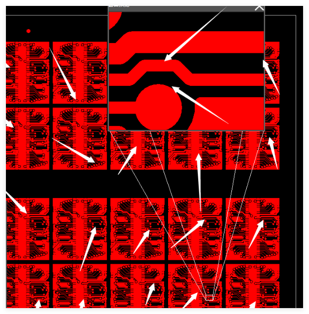
Would you mind setting your min trace spacing to .103mm please. The last boards I had to change a bit as the boardhouse complained some parts were <.1mm I don't think you did anything wrong. I checked and DRC was clean...
Avatar
I guess the one thing I haven't considered yet is whether I can connect all the grounds, but hopefully I'll work something out 😄
😂 1
Avatar
haha, if it has to be 4 I don't think that's the end of the world, and if that's the case you can also disregard the previous statement.
10:40 p.m.
4layer spec is .09 so we're all clear there.
Avatar
Will do. Also for the last one I had hole to hole 0.25mm, but I double checked the JLC rules and they are 0.2 so I tuned that down to 0.2, does that sound ok? Maybe should put a safety fudge on that too?
Avatar
Wouldn't hurt. Again, I have no idea why they failed us. let me get the pic, 1 sec
10:43 p.m.
This was what they sent us.
Avatar
Hmm, was the problem via to track?
Avatar
4 layer is also an easy fix. Also I have no idea, there are arrows everywhere it seems 🤣
😆 1
10:45 p.m.
Hi there, Sorry to bother you, but we'd like to confirm with you an issue found when engineer making production file of your PCB order. The spacing between traces is smaller than 0.1mm which is not enough to proceed, could we help you cancel this order?
Avatar
Weird, maybe some unit conversion caused some rounding issue? Anyway, I'll go up to 0.103 - I've got a bunch of tightly packed traces but hopefully won't take too long to wiggle them apart!
10:50 p.m.
Cool, and good to know that 4 layer isn't a major issue - if we end up trying to do custom CoBs to match important pins on all the Racquet and TinyQV designs then routing might get even more fun!
10:53 p.m.
Anyway - I need to call it a night - I've pushed my WIP to https://github.com/MichaelBell/chip-on-board-wire-bonded-pcbs/tree/half-slot-dev if you want to take a look
Wire bonded chip on board PCB designs. Contribute to MichaelBell/chip-on-board-wire-bonded-pcbs development by creating an account on GitHub.
Avatar
Avatar
RebelMike
Anyway - I need to call it a night - I've pushed my WIP to https://github.com/MichaelBell/chip-on-board-wire-bonded-pcbs/tree/half-slot-dev if you want to take a look
Thanks and goodnight
Avatar
Avatar
Andrew Wingate
haha, if it has to be 4 I don't think that's the end of the world, and if that's the case you can also disregard the previous statement.
Are you doing JLC? If so, I'd be surprised why you weren't just going for 4L in the first place.
Avatar
Avatar
namibj
Are you doing JLC? If so, I'd be surprised why you weren't just going for 4L in the first place.
We are. That's why I was saying that as well. It's not much difference in price
Avatar
Yeah 4L for signal integrity!
Avatar
That as well
Avatar
In the interest of possibly understanding safety margins that were shown to not be that large by Tholin's DAC's OpAmps, do we have material datasheet information or enough detail that I could dig such up for the COBs? Notably, thermal expansion behavior of the board; how the chip is attached to the board; what the goop is that's covering the front of the die.
Avatar
So I was thinking - if the plan is to do custom CoB PCBs for TinyQV and the other run 1 half slot designs, then why are we trying to match the pinout for the default template on the generic half slot CoBs? It would be better just to do the natural pinout and then fix the templates, rather than doing more complex than necessary routing and then locking that in for future runs. It would also make sense to update all the CoBs to 4 layer for better signal integrity if the cost difference is negligible. That does obviously require the generic CoBs are completed reasonably quickly so that the template can be updated in plenty of time for the run 2 designs. But I wouldn't suggest moving any of the power pads, clock or reset, and beyond that it is likely that pinout matching only matters if people are submitting the same design at different slot sizes, or expecting a common motherboard to work between different slot sizes on the basis of using pins with the same name in the template. Thoughts?
Avatar
Avatar
RebelMike
So I was thinking - if the plan is to do custom CoB PCBs for TinyQV and the other run 1 half slot designs, then why are we trying to match the pinout for the default template on the generic half slot CoBs? It would be better just to do the natural pinout and then fix the templates, rather than doing more complex than necessary routing and then locking that in for future runs. It would also make sense to update all the CoBs to 4 layer for better signal integrity if the cost difference is negligible. That does obviously require the generic CoBs are completed reasonably quickly so that the template can be updated in plenty of time for the run 2 designs. But I wouldn't suggest moving any of the power pads, clock or reset, and beyond that it is likely that pinout matching only matters if people are submitting the same design at different slot sizes, or expecting a common motherboard to work between different slot sizes on the basis of using pins with the same name in the template. Thoughts?
Andrew Wingate 2026-05-21 9:48 p.m.
I've been speaking with @Tim 'mithro' Ansell and have been wanting to change things about the layout and the standard template and fix things at the beginning so it's harmonized across the sizes from the start.
Avatar
Cool, it probably wouldn't take long to work out what the natural pad order would be and adjust the default template, even if the routing isn't actually done at that point. I know @Leo Moser (mole99) is planning to push a significant template update soon so if that is the direction maybe getting it done before that goes out would be a good idea
👍 1
Avatar
Avatar
namibj
In the interest of possibly understanding safety margins that were shown to not be that large by Tholin's DAC's OpAmps, do we have material datasheet information or enough detail that I could dig such up for the COBs? Notably, thermal expansion behavior of the board; how the chip is attached to the board; what the goop is that's covering the front of the die.
Tim 'mithro' Ansell 2026-05-22 1:20 a.m.
I'm sure a professional packaging house will happily provide you with all these details if you are willing to order at least 1 million units a month. For $1.50 USD for <1000 units getting things like data sheets is pretty impossible most of the time.
Avatar
Avatar
RebelMike
Cool, it probably wouldn't take long to work out what the natural pad order would be and adjust the default template, even if the routing isn't actually done at that point. I know @Leo Moser (mole99) is planning to push a significant template update soon so if that is the direction maybe getting it done before that goes out would be a good idea
Leo Moser (mole99) 2026-05-22 6:22 a.m.
I agree, we should probably do all of the major changes now, so people only need to migrate once. @Andrew Wingate we should also change the pin order of the die to match the CoB, so that it doesn't need to be turned upside down. This should help reduce the confusion around the pinout, too.
Avatar
Why not just rotate the CoB PCB by 180 deg ... ?
Avatar
The pin number themselves already match, it's just on the PCB version / footprint, it was rotated so the first is on the top right instead of bottom left ...
Avatar
Leo Moser (mole99) 2026-05-22 8:13 a.m.
I thought there was a reason downstream why that isn't easily possible. @Andrew Wingate what was the reason again for rotating the die? Perhaps we should just change the PCB then. In any case, it should be consistent.
Avatar
Andrew Wingate 2026-05-22 6:57 p.m.
@tnt @Leo Moser (mole99) Just rotating won't fix the underlying problem. We should strive to harmonize default across the different die sizes. If we follow something like my diagrams here, you could design for any size die and still get a cob that matches all three (or four if the 1/4 slot follows) I prefer the fiducial to be up top because it follows convention
Avatar
I think the thing that made it confusing is that the die has a wafer.space logo on it and the PCB has a waver.space logo on it, but they are on opposite corners from each other
7:00 p.m.
Instead of it being used as a alignment marker
Avatar
Andrew Wingate 2026-05-22 7:01 p.m.
Agreed that did not help. Not sure how it's getting announced, but if you want to have the COB 3 corners will be used by the defaults. Qr code, ws logo, blank space. The Qr and the blank will be in opposing corners
Avatar
@Andrew Wingate The current COB footprint on the PCB has the pad 0 in the top right, not top left ... so if you rotate it 180 it's fine and aligned with the die.
Avatar
Avatar
tnt
@Andrew Wingate The current COB footprint on the PCB has the pad 0 in the top right, not top left ... so if you rotate it 180 it's fine and aligned with the die.
Andrew Wingate 2026-05-22 7:30 p.m.
That is correct
Avatar
That was the main issue in assmbly ... people expected the die to be placed in the same way it was visible in the GDS.
Avatar
Avatar
tnt
That was the main issue in assmbly ... people expected the die to be placed in the same way it was visible in the GDS.
Andrew Wingate 2026-05-22 7:34 p.m.
I believe what we have here is an x y problem To me, I think harmonizing across the die sizes is the bigger issue. If you're changing that, then also change the position of the fiducial so it cannot be confused.
The XY problem is a communication problem encountered in help desk, technical support, software engineering, or customer service situations where the question is about an end user's attempted solution (X) rather than the root problem itself (Y). The XY problem obscures the real issues and may even introduce secondary problems that lead to miscom...
Avatar
I think there are just two independent issues that should be addressed at the same time:
  • The CoB layout for half and quarter slots isn't finalised (and wasn't known when run 1 designs were done), so projects in different size slots can't match their pinouts. Once the layout is known it would make sense to harmonize the default template (but most people will customize that anyway, so the important thing is knowing the mapping).
  • The wafer space logos are in different places on the board and the chip, which is confusing. The proposal seems to be to change both board and template to have the logo (and therefore pin 1) in the top left, is that correct? Obviously everyone will need to update their run 2 projects if that change is made.
Avatar
Avatar
RebelMike
I think there are just two independent issues that should be addressed at the same time:
  • The CoB layout for half and quarter slots isn't finalised (and wasn't known when run 1 designs were done), so projects in different size slots can't match their pinouts. Once the layout is known it would make sense to harmonize the default template (but most people will customize that anyway, so the important thing is knowing the mapping).
  • The wafer space logos are in different places on the board and the chip, which is confusing. The proposal seems to be to change both board and template to have the logo (and therefore pin 1) in the top left, is that correct? Obviously everyone will need to update their run 2 projects if that change is made.
Andrew Wingate 2026-05-23 6:12 p.m.
Agreed, and thanks for the work you've done with the half slot dies. And to be clear, a lot of the changes I'm requesting are still just my opinion. That said, having worked with a number of the downstream effects, someday we're likely to want to make changes. Harmonizing the template across sizes will help with whatever next version of cob we may introduce, if people want to harmonize across different dip like packages, this would be easier. Unless I'm mistaken, I think we collectively have enough information to make some better decisions across the board. And doing so sooner than later would be better.
👍 1
6:18 p.m.
Also of note, any of these propositions are only for people who are looking to get the standard COB packaging. Other than that, anyone's still free to do whatever they like.
Avatar
On the half slot CoBs, I’ve now got distracted by a possible run 2 silicon project, but I could potentially do some more on those.
Avatar
Andrew Wingate 2026-05-23 6:21 p.m.
The first panels of the p5x1 version should be back from the board house in the next few days if I understand correctly
👍 1
Avatar
CoB work items I'm aware I could look at:
  • Make a simplified version of the 1x0p5 CoB, and also going up to 4 layers. That would become the standard one going forwards
  • Have another go at the 0p5x1 - this time going for the simplest routing, and hence probably just having the chip in the obvious "upright" position rather than diagonal. Again change to 4 layers.
  • Create run 1 TinyQV specific 1x0p5, 0p5x1 (and eventually 0p5x0p5) CoBs that match clk, SPI, UART to the pinout of the 1x1 GD03 Racquet project.
(edited)
6:27 p.m.
Then there's:
  • Create a motherboard against that pinout that could be used by TinyQV or Racquet with the custom CoB
  • And also make a TinyQV motherboard for the original 1x0p5 CoB, if I'm likely to receive any chips bonded to it 🙂
6:28 p.m.
I would ideally like to get my hands on a TinyQV board a little before the run 2 deadline as I may be doing a revision so it would be good to know if anything didn't work (edited)
Avatar
Andrew Wingate 2026-05-23 6:33 p.m.
And also make a TinyQV motherboard for the original 1x0p5 CoB, if I'm likely to receive any chips bonded to it
As far as I understand, this is definitely the plan. I can't imagine it's not. I'm not in China anymore so am a bit more detached now. I would bet something gets sent to you in about a week or two.
Avatar
Avatar
Andrew Wingate
And also make a TinyQV motherboard for the original 1x0p5 CoB, if I'm likely to receive any chips bonded to it
As far as I understand, this is definitely the plan. I can't imagine it's not. I'm not in China anymore so am a bit more detached now. I would bet something gets sent to you in about a week or two.
Awesome! There's two copies of TinyQV in this size slot so even if Tim would like a bunch in a custom CoB eventually there should be loads left still. I'll put together a quick motherboard based on the pinout on the existing CoB so I have something to test with.
💜 1
Avatar
Just to double check, is this the correct part for the mating connector? https://www.lcsc.com/product-detail/C19089292.html
HC-PBB40C-70DS-0.4V-3.0-02 by HCTL - In-stock components at LCSC. Price from $0.3911. Free access HC-PBB40C-70DS-0.4V-3.0-02 datasheet, Package, pinout diagrams, and BOM tools.
7:17 p.m.
The link from the https://github.com/wafer-space/chip-on-board-wire-bonded-pcbs/ readme is broken (maybe the part number has changed?)
Avatar
Avatar
RebelMike
Just to double check, is this the correct part for the mating connector? https://www.lcsc.com/product-detail/C19089292.html
Andrew Wingate 2026-05-23 7:18 p.m.
That is correct. Keep in mind there are a number of different heights if that is of concern, and there are also other compatible brands as well.
👍 1
Avatar
Avatar
RebelMike
The link from the https://github.com/wafer-space/chip-on-board-wire-bonded-pcbs/ readme is broken (maybe the part number has changed?)
Andrew Wingate 2026-05-23 7:20 p.m.
The link has been fixed. Thanks
👍 1
Avatar
Doh. Just finished routing my board. For some reason at that point I decided to double check that the pinout of the mezzanine connector was correct. And it's not - the pins on the connector in the motherboards project which I grabbed the footprint from are flipped compared to the CoB! That doesn't matter for those simple breakouts because they just expose all the pins. Incidentally I think that means the pin 1 marking on those simple breakout motherboards is actually against pin 70.
Avatar
Ah, this is the same thing that @BreakingTaps spotted last week!
🫠 1
Leo Moser (mole99) started a thread. 2026-05-24 10:55 a.m.
Avatar
Andrew Wingate 2026-05-24 5:48 p.m.
Hey @Leo Moser (mole99) stuff seems to get lost in threads on discord. For starters, I don't think any of this 'should' happen for run2. I think it's too late for that.
I'm not exactly sure what your diagram is showing?
I just decided to make a rough thing to illustrate. @RebelMike you could probably imagine a ring of vias that do whatever on the bottom side, but all route cleanly on the top.
I agree that we should harmonize what we can between the different slots sizes. What are your plans with regards to matching the pinout?
If we want to keep that many pins on all the half slots and drop 2 from the 1x1 we end up with them all being identical. I don't know what this means in reality, but if someone wanted to prototype on a half slot, then move to a larger size, the pin/padout stays identical.
PS: Looking at the CoB PCB for the 1x1 slot, pin 1 of the mezzanine connector seems to be in the top right corner rather than the top left. Why is that the case?
KiCads generic connector library and most packages and connectors in general have pin1 in the top left. I would prefer, if someone were to take a generic mezzanine connector and use the footprint provided by the manufacturer, for pin1 to line up. There's already a lot of confusion when trying to go through all these maps to add one more translation.
Avatar
But connectors is on the bottom of the PCB, opposite of die. And then the connector on the "user side" is also swapped because it's the other side of the connection ... they can't be all top left pin 1 footprint, at some point swap needs to occur ... (edited)
Avatar
Avatar
tnt
But connectors is on the bottom of the PCB, opposite of die. And then the connector on the "user side" is also swapped because it's the other side of the connection ... they can't be all top left pin 1 footprint, at some point swap needs to occur ... (edited)
Andrew Wingate 2026-05-24 6:20 p.m.
Agreed, when mentioning the connector above, I was referring to the connector a user would be sourcing (on their motherboard). The important one in my mind is the final connector and the die itself to match. (edited)
Avatar
But the "manufacturer footprint" argument doesn't hold really. If you look at the kicad library ( in the Hirose library for DF12 that's the closest I have installed ), the DS side connector which would be the "user side" , they standardized indeed on pin 1 top left ... with the connector horizontal. Which means top right if you put it vertically ( or bottom left ) ...
Avatar
Andrew Wingate 2026-05-24 6:51 p.m.
Whatever, I'm not religious about this. Seems like others are. I also tend to make and throw a bunch of stuff against the wall to see what sticks. More to the point of harmonizing. There is an error in my pictures from the last post. I am reposting more correct versions. I have also created an example slot_size.yaml thing. I am not sure how many people will be designing for multiple slot sizes, or how difficult that is. @RebelMike can maybe speak to that. In the spirit of making more things, I propose a config that has a different shape. There is a single list of pads that doesn't change between slot sizes.
6:52 p.m.
And for the record I am aware this obscures a starting pad even further
Avatar
IMO what needs to be clear and uniform across all 3 slabs of multilayer routing is that there's exactly one clear orienting corner, and they all line up when assembled correctly. Die, COB, motherboard's socket area.
👍 2
7:28 p.m.
That's easy to verify when looking at a layout and picking like 3-ish nets to highlight and visually check. The top surface of all 3 is the same "up".
👍 2
Avatar
Avatar
namibj
That's easy to verify when looking at a layout and picking like 3-ish nets to highlight and visually check. The top surface of all 3 is the same "up".
(in the sense of surface-normal-vector direction)
Avatar
I was assuming power pads would stay where they were and this was simply an exercise in renaming the signal pads in the default template on the half (and quarter) slots. That basically has no implications except for helping make the CoB pinout clearer as there would be a single mapping default template -> pins, which projects could compare their renamed pins against. But for run 3 obviously bigger changes could be considered - I'm not clear on what the implications of removing two power pads from the 1x1 pad ring would be.
Avatar
Don't remove too many power pads, at least if we have a way to not fry chips as much as the avalon Run1 DACs are doing.
8:20 p.m.
larger chip more consumption
Avatar
My thoughts:
  • The wafer space logos should be in the same position as it's the obvious marker to align in assembly (I'd weakly suggest top right as aesthetically it looks most pleasing there - Andrew and Leo both put it there independently AFAICT) - this doesn't necessarily need to mean "pin 1".
  • To allow that without users having to change their run 2 designs, the CoB pinout should be changed (this would likely end up ~a 180 degree rotation on the current pinout, and maybe if it could be exactly that that would leave some compatibility between run 1 and run 2).
  • The project pad -> mezzanine pin mapping should be clearly documented, with reference to the pad names in the default template and the pin names on the mezzanine footprint for the user's motherboard.
  • The signal (and VDD?) pins on the default templates should be harmonized as much as possible, so the above documentation applies to all slot sizes Ideally that should be done for run 2, because the current state is a source of confusion and mistakes.
8:24 p.m.
On the pin types in the templates, I suspect it would make sense to keep some analog and input ones to highlight their existence in the template, rather than just making everything bidir. My principle of least change was suggesting make everything match the current 1x1 but that does have quite a large number of dedicated inputs
Avatar
Andrew Wingate 2026-05-24 8:28 p.m.
Think of all these as conceptual models rather than genuine proposals. More power pins are perfectly acceptable. An overarching goal expressed by @Tim 'mithro' Ansell is to look for ways to reduce cost in efforts towards accessibility. This likely means moving away from the mezzanine all together, and taking any decoupling caps with it, since assembly is no longer an operation we're doing. No caps means more pins can be used for whatever purpose as they all become generic wires.
Avatar
Yeah it's a good top right corner "arrow"
8:30 p.m.
8:30 p.m.
qr code lacks coarse structure contrast
8:31 p.m.
W.S logo or alternatively (if for some reason that has to not be there) an Intel LGA style triangle should be strongly recommended.
8:32 p.m.
(The QR would work if the other corners were blank, but they aren't.)
Avatar
Avatar
RebelMike
My thoughts:
  • The wafer space logos should be in the same position as it's the obvious marker to align in assembly (I'd weakly suggest top right as aesthetically it looks most pleasing there - Andrew and Leo both put it there independently AFAICT) - this doesn't necessarily need to mean "pin 1".
  • To allow that without users having to change their run 2 designs, the CoB pinout should be changed (this would likely end up ~a 180 degree rotation on the current pinout, and maybe if it could be exactly that that would leave some compatibility between run 1 and run 2).
  • The project pad -> mezzanine pin mapping should be clearly documented, with reference to the pad names in the default template and the pin names on the mezzanine footprint for the user's motherboard.
  • The signal (and VDD?) pins on the default templates should be harmonized as much as possible, so the above documentation applies to all slot sizes Ideally that should be done for run 2, because the current state is a source of confusion and mistakes.
Andrew Wingate 2026-05-24 8:36 p.m.
I think all that sounds reasonable.
The project pad -> mezzanine pin mapping should be clearly documented, with reference to the pad names in the default template and the pin names on the mezzanine footprint for the user's motherboard.
I'm finally getting settled as I get home and plan to work on cleaning the repo with the current COB and better document the motherboard. I think that will take away most of the confusion.
The wafer space logos should be in the same position as it's the obvious marker to align in assembly (I'd weakly suggest top right as aesthetically it looks most pleasing there - Andrew and Leo both put it there independently AFAICT) - this doesn't necessarily need to mean "pin 1".
The one request I did have, is whatever corner we are using as 'fiducial' has the opposing corner blank. This could happen this run, or not.
To allow that without users having to change their run 2 designs, the CoB pinout should be changed (this would likely end up ~a 180 degree rotation on the current pinout, and maybe if it could be exactly that that would leave some compatibility between run 1 and run 2).
I don't understand this one fully? Basically rotate all the copper 180? That would do it? (negating changes to the schematic)
The signal (and VDD?) pins on the default templates should be harmonized as much as possible, so the above documentation applies to all slot sizes
This is a run3 thing?
8:39 p.m.
The signal (and VDD?) pins on the default templates should be harmonized as much as possible, so the above documentation applies to all slot sizes
I think I see. When making all this I did not have that info. I've been filling in this spreadsheet as I got more info https://docs.google.com/spreadsheets/d/1pI2BAEWEexXcXN3vah3SR85zPIV6eAXPGXc2bcvoSGU/edit?gid=0#gid=0 You're saying to use the info in the config.yaml column?
Avatar
Avatar
Andrew Wingate
I think all that sounds reasonable.
The project pad -> mezzanine pin mapping should be clearly documented, with reference to the pad names in the default template and the pin names on the mezzanine footprint for the user's motherboard.
I'm finally getting settled as I get home and plan to work on cleaning the repo with the current COB and better document the motherboard. I think that will take away most of the confusion.
The wafer space logos should be in the same position as it's the obvious marker to align in assembly (I'd weakly suggest top right as aesthetically it looks most pleasing there - Andrew and Leo both put it there independently AFAICT) - this doesn't necessarily need to mean "pin 1".
The one request I did have, is whatever corner we are using as 'fiducial' has the opposing corner blank. This could happen this run, or not.
To allow that without users having to change their run 2 designs, the CoB pinout should be changed (this would likely end up ~a 180 degree rotation on the current pinout, and maybe if it could be exactly that that would leave some compatibility between run 1 and run 2).
I don't understand this one fully? Basically rotate all the copper 180? That would do it? (negating changes to the schematic)
The signal (and VDD?) pins on the default templates should be harmonized as much as possible, so the above documentation applies to all slot sizes
This is a run3 thing?
The one request I did have, is whatever corner we are using as 'fiducial' has the opposing corner blank. This could happen this run, or not.
The location is specified in the project's config, but I assume is validated by the submission system, so changing it and then advising people of the change should be possible?
Basically rotate all the copper 180? That would do it? (negating changes to the schematic)
Yeah I think rotating everything through 180 but leaving the logo where it is would resolve it.
You're saying to use the info in the config.yaml column?
Yes - while users will rename their pins, they will have started from this setup so it seems the most meaningful thing to me. Maybe I'm putting too much weight on it though
Avatar
Andrew Wingate 2026-05-24 8:45 p.m.
Can you explain the reason they may be called bidir\\[0\\].pad and inputs\\[0\\].pad instead of something more generic if it's just overwritten anyways?
8:49 p.m.
Users may well change those to match their needs, but given wafer space is providing both the project template and the CoB, referring to things by those names seems like it should make sense to people
👍 1
8:52 p.m.
In my case, I was short on time and also didn't know what slot size you might have going spare, so I just fitted my design in to the template without changing any of the pad names. Then you had spare slots of all half and quarter sizes so all 3 got produced! That's what led to me wishing that the default pinout was harmonized back in run 1. That's probably a pretty unique circumstance though so I think going forwards its more about documentation, but it would also reduce surprises if you do switch which slot you're targetting.
Avatar
Avatar
RebelMike
Users may well change those to match their needs, but given wafer space is providing both the project template and the CoB, referring to things by those names seems like it should make sense to people
Andrew Wingate 2026-05-24 8:57 p.m.
I'm going to go out on a limb and say I don't think switching slot sizes will be all that uncommon in the future. More or less I think things are pretty entrenched as far as run1 goes. I'll try to make the changes listed above. I would like to keep the conversation alive about run3 though. Thanks for the input
👍 1
Avatar
oh, hmmmmm..... @BreakingTaps any hope for the idea of using ACF and DRC-pushed FPC (JLC just about lets you do 102 um pitch on the 5$ special)? Or is that too high resistance/would need fancy surface treatment on the die to connect to the aluminium topmetal? I'd expect AOI to reject even up to half the FPC production to be sufficiently practical to work from that POV; but it's not easy to find out if the commodity ACF would have sufficient performance to do the task of W.S default/bargain fan-out. It is my understanding that the traces are on top of the core and the lack of fine-pitch coverlay/soldermask would imply that these are bare metal strips on an underlying flat polyimide core; so that might be enough "bump"? It's about 12um thick there.
Avatar
Ok I'll draw up a standard COB pinout FPC for that tomorrow. This.... might just work.
Avatar
Avatar
namibj
Ok I'll draw up a standard COB pinout FPC for that tomorrow. This.... might just work.
What is this?
Avatar
Avatar
Andrew Wingate
What is this?
https://www.youtube.com/watch?v=0HZ35CyHVxQ https://web.archive.org/web/20190708182030/https://fsrkj.com/upfiles/201712/22/af0aa1f1cb2886b6f.pdf It's on aliexpress for like 7 USD a roll; seems to not be hard to get one's hands on, and it's just 190±10 C for 10 s at 2 MPa via a hard-ish silicone sheet (200~300 um they say, shore 70+) with a thn teflon sheet (25~50 um) between that and the FPC, pressing the contact strip area down using a sufficciently solid anvil underneath to not harm the more-fragile die (or, in the original case, the LCD's glass; it works for dies too, though, "just" not well on aluminium at least with that standard metallurgy)
Avatar
Avatar
namibj
https://www.youtube.com/watch?v=0HZ35CyHVxQ https://web.archive.org/web/20190708182030/https://fsrkj.com/upfiles/201712/22/af0aa1f1cb2886b6f.pdf It's on aliexpress for like 7 USD a roll; seems to not be hard to get one's hands on, and it's just 190±10 C for 10 s at 2 MPa via a hard-ish silicone sheet (200~300 um they say, shore 70+) with a thn teflon sheet (25~50 um) between that and the FPC, pressing the contact strip area down using a sufficciently solid anvil underneath to not harm the more-fragile die (or, in the original case, the LCD's glass; it works for dies too, though, "just" not well on aluminium at least with that standard metallurgy)
I've seen this video before. Super neat!! Good luck!
Avatar
Avatar
Andrew Wingate
I've seen this video before. Super neat!! Good luck!
yeah same I remembered didn't even remember it was him but tbf, fits.
Avatar
Avatar
namibj
oh, hmmmmm..... @BreakingTaps any hope for the idea of using ACF and DRC-pushed FPC (JLC just about lets you do 102 um pitch on the 5$ special)? Or is that too high resistance/would need fancy surface treatment on the die to connect to the aluminium topmetal? I'd expect AOI to reject even up to half the FPC production to be sufficiently practical to work from that POV; but it's not easy to find out if the commodity ACF would have sufficient performance to do the task of W.S default/bargain fan-out. It is my understanding that the traces are on top of the core and the lack of fine-pitch coverlay/soldermask would imply that these are bare metal strips on an underlying flat polyimide core; so that might be enough "bump"? It's about 12um thick there.
oh that's a fun idea! I'm not sure to be honest, might be dodgy for high frequency signals, but maybe fine for less demanding tasks? I dont actually have much experience with the stuff on real projects, just tearing down existing projects to get to the ACF for microscopy 🙂 But yeah it's used all over for displays Could be a really clever way to get flipchip without needing the fab to bump for us!
🔥 1
Avatar
Avatar
BreakingTaps
oh that's a fun idea! I'm not sure to be honest, might be dodgy for high frequency signals, but maybe fine for less demanding tasks? I dont actually have much experience with the stuff on real projects, just tearing down existing projects to get to the ACF for microscopy 🙂 But yeah it's used all over for displays Could be a really clever way to get flipchip without needing the fab to bump for us!
It's actually waaaay better for high frequency it's a bit resistive but I'm sure that's easy to tune away in a transceiver as we talk like a couple Ohm at the terminus. That 3mm bond wire at 1 GHz is already 12 ohm though... If you have any idea how to get some test dies receptive to the nickel spheres....
Avatar
ah interesting, why would more resistance help with higher frequency? I sorta assumed you'd want the shortest, most conductive path possible?
6:55 p.m.
our topmetal is aluminum right? I just skimmed that old video of mine and they used Al on the glass connector side. So it was Al -> ACF -> Ni/P coated Cu fpc
Avatar
Avatar
BreakingTaps
our topmetal is aluminum right? I just skimmed that old video of mine and they used Al on the glass connector side. So it was Al -> ACF -> Ni/P coated Cu fpc
Andrew Wingate 2026-05-25 6:56 p.m.
As far as I understand, yes, it's aluminum.
👍 1
Avatar
Avatar
BreakingTaps
ah interesting, why would more resistance help with higher frequency? I sorta assumed you'd want the shortest, most conductive path possible?
It's easier to control resonances with slight dampening. You lose a bit of Q but you get a more consistent response
👍 2
Avatar
gotcha, TIL!
Avatar
Avatar
BreakingTaps
ah interesting, why would more resistance help with higher frequency? I sorta assumed you'd want the shortest, most conductive path possible?
It's got comparatively zero inductance once you include the remaining parasitics.
Avatar
Avatar
BreakingTaps
our topmetal is aluminum right? I just skimmed that old video of mine and they used Al on the glass connector side. So it was Al -> ACF -> Ni/P coated Cu fpc
Wait they they.... They did Al straight to the ACF??? I'll get you a JLC special FPC layout/pinout for your die before the weekend if you'd be interested in trying.
Avatar
Avatar
Christopher
It's easier to control resonances with slight dampening. You lose a bit of Q but you get a more consistent response
Well it's more that you can tune the launch impedance a bit anyways once it matters and that'll easily cover the spread in series resistance from the ACF. Like you already need the structures in the PA (yeah it's digital but it's still a power amplifier, with tuned distortion, and sometimes integrally fused modulator if the output itself is naturally clocked instead of being a second stage after the clocked stage) and a bit more tuning range to cover increased stacking of variance is not really expensive at that point. So therefore you might as well just enjoy the much lower inductance.
4:11 a.m.
If you have any special wishes on that provide a schematic. I'd plan for having the mezzanine connector off the side so you could bend it and have the entire thing barely taller/thicker than the original cob, but now with the die backside exposed to attach a heatsink. I'd probably do it on Thursday early Berlin time; if that's too early I'd get to it approximately a week later (that's Germanys closest thing to a comiket this coming weekend I'll be running on fumes by the end).
Avatar
Avatar
namibj
Wait they they.... They did Al straight to the ACF??? I'll get you a JLC special FPC layout/pinout for your die before the weekend if you'd be interested in trying.
Tim 'mithro' Ansell 2026-05-26 8:59 a.m.
What does ACF stand for?
Avatar
Tim 'mithro' Ansell 2026-05-26 9:01 a.m.
ACF is the tape stuff that @BreakingTaps is talking in the video you shared?
Avatar
Avatar
Tim 'mithro' Ansell
ACF is the tape stuff that @BreakingTaps is talking in the video you shared?
Yeah
9:02 a.m.
It's what they use to bond to notably LCDs and other TFT-on-glass type active-matrix displays like OLED.
9:03 a.m.
It's a 180~190C for 2~10 seconds thermoset epoxy used with about 2MPa pressure.
Avatar
"Anisotropic Conductive Film" yep
Avatar
Avatar
namibj
Wait they they.... They did Al straight to the ACF??? I'll get you a JLC special FPC layout/pinout for your die before the weekend if you'd be interested in trying.
At least for the glass-FPC interface, looks that way. Copper FPC pad on top, glass on bottom. Thin film of aluminum on glass side. (please excuse my shitty cross-section polishing I was in a rush 😄 ) Edit: also ignore the silver, iirc I sputtered a very thin layer on to help with charging on the glass (edited)
😍 1
Avatar
I did a quick tweak to the generic breakout to make it 4 layer and label clk/rst/power/ground - don't know if this would be useful to anyone else: https://codeberg.org/rebelmike/ws-breakout
👍 2
Avatar
Avatar
RebelMike
I did a quick tweak to the generic breakout to make it 4 layer and label clk/rst/power/ground - don't know if this would be useful to anyone else: https://codeberg.org/rebelmike/ws-breakout
Tim 'mithro' Ansell 2026-05-29 4:40 a.m.
Cool!
Avatar
Andrew Wingate 2026-05-30 3:36 a.m.
Hey all, I've added and updated some of the readmes and moved all the run-1 stuff into it's own directory so we can keep things more organized moving forward. https://github.com/wafer-space/chip-on-board-wire-bonded-pcbs This likely breaks any way for you to make pull requests Mike. side note- this has the updated 1xp5 files that have the larger clearance. @Tim 'mithro' Ansell @RebelMike
Wire bonded chip on board PCB designs. Contribute to wafer-space/chip-on-board-wire-bonded-pcbs development by creating an account on GitHub.
waferspace 1
3:37 a.m.
Also updated the motherboards to have these as the symbols.
🎉 2
❤️ 1
Exported 238 message(s)
Timezone: UTC+0