wafer.space Community
📐 - Designing / 📦-cob
Channel for discussing chip-on-board packaging options for wafer.space bare die.
Between 2026-08-31 11:59 p.m. and 2026-10-01 12:00 a.m.


 1


 2
 1

 2
 1 1
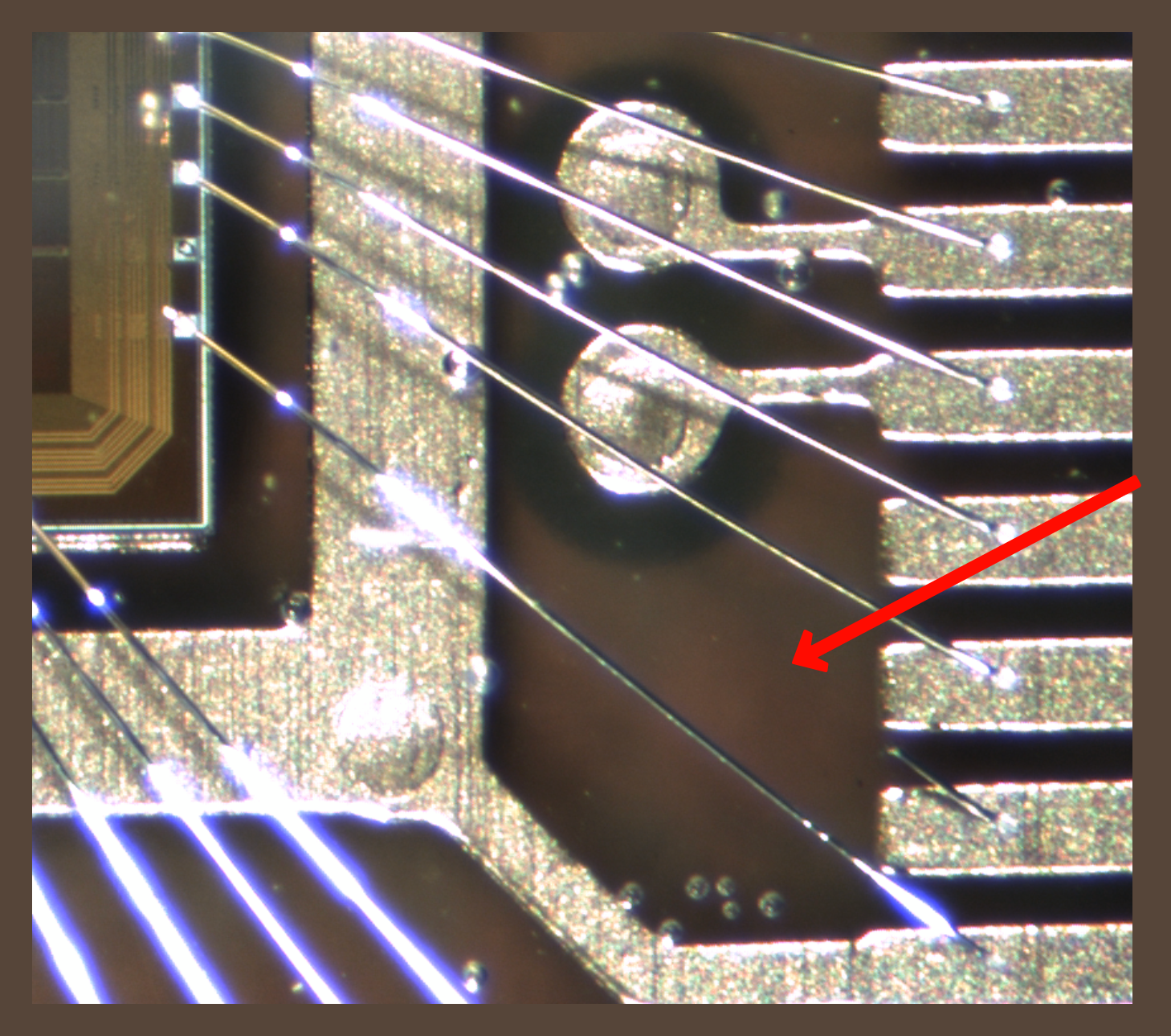
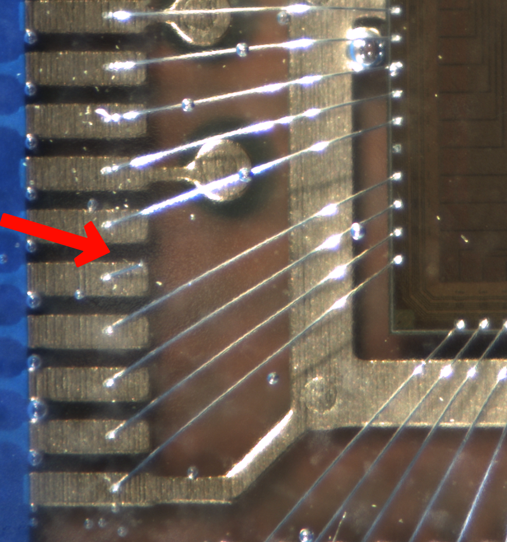
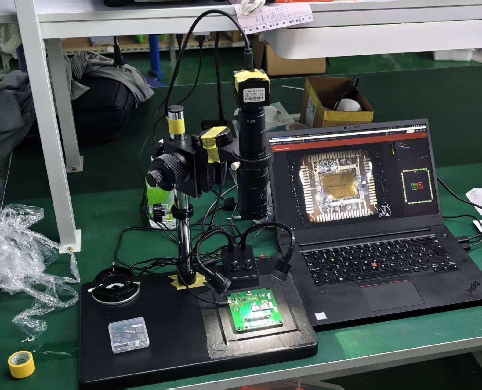
 Bond tester update: smarter, more die-agnostic testing
Sorry for the long post.
TLDR
 . But let's try to leave that to next year. For our simple pass/fail testing, the current setup does the job.
Power pads: capacitor charging curve
Power pins used to cause trouble because of the decoupling capacitors on the PCB. Instead of fighting that, the tester now measures the charging curve itself: a good bond connects the pad to the die, whose ESD diode clamps the voltage before the capacitor charges fully. An open bond has no such clamp and lets it charge to full.
What's next
I expect there are still plenty of surprises waiting once we start bonding more CoBs. So far I've only managed to test a handful of different dies, and with new upcoming CoBs I expect the tool to fail in new ways, which is a good thing: every failure shows how to make the tester better and more universal.
Once the run 1 CoBs are done, we should be in a good position for an updated PCB design. Longer term, I'd like to keep improving the tester, with upgrading the current sources and the ADC at the top of the list.
If you have any questions or suggestions, please feel free to leave a reply
 1
 1
 1

 1


 1
 I think the pad config script that removes unused edges is all merged into the template now so it should just happen automatically if you remove all the pins from the three unwanted sides.
However, as is this leaves the corners adjacent to the used edge in place, so might not be exactly what you want. (edited)
 1
 1 1 1
 1 Bond tester update: smarter, more die-agnostic testing
Sorry for the long post.
TLDR. But let's try to leave that to next year. For our simple pass/fail testing, the current setup does the job.
Power pads: capacitor charging curve
Power pins used to cause trouble because of the decoupling capacitors on the PCB. Instead of fighting that, the tester now measures the charging curve itself: a good bond connects the pad to the die, whose ESD diode clamps the voltage before the capacitor charges fully. An open bond has no such clamp and lets it charge to full.
What's next
I expect there are still plenty of surprises waiting once we start bonding more CoBs. So far I've only managed to test a handful of different dies, and with new upcoming CoBs I expect the tool to fail in new ways, which is a good thing: every failure shows how to make the tester better and more universal.
Once the run 1 CoBs are done, we should be in a good position for an updated PCB design. Longer term, I'd like to keep improving the tester, with upgrading the current sources and the ADC at the top of the list.
If you have any questions or suggestions, please feel free to leave a reply 1 1 1


 1
 so yeah 5x5mm it is
 2
 1 (edited)

 1 1


 3 1

 I think it was just HaD europe and IIUC correcly we'll give extra left over to people at ORConf. 1 2 1
 1


 4 1
<xxx>.cob.json file workflow for documenting bonding parameters and EDA landpatterns 1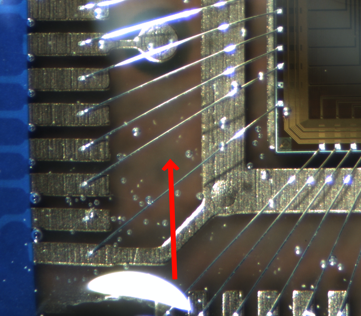
 1
(1/e²) beam divergence is given at 18° typ 25° max and reading the intensity plot in the datasheet the full width half maximum is about 8.5°), so I could try to approximately target having an on-die photodiode good for fiber data communications with a suitable low cost VCSEL diode transmitter. Notably vague ideas of brightness and less vague ideas of beam size and spectrum matter.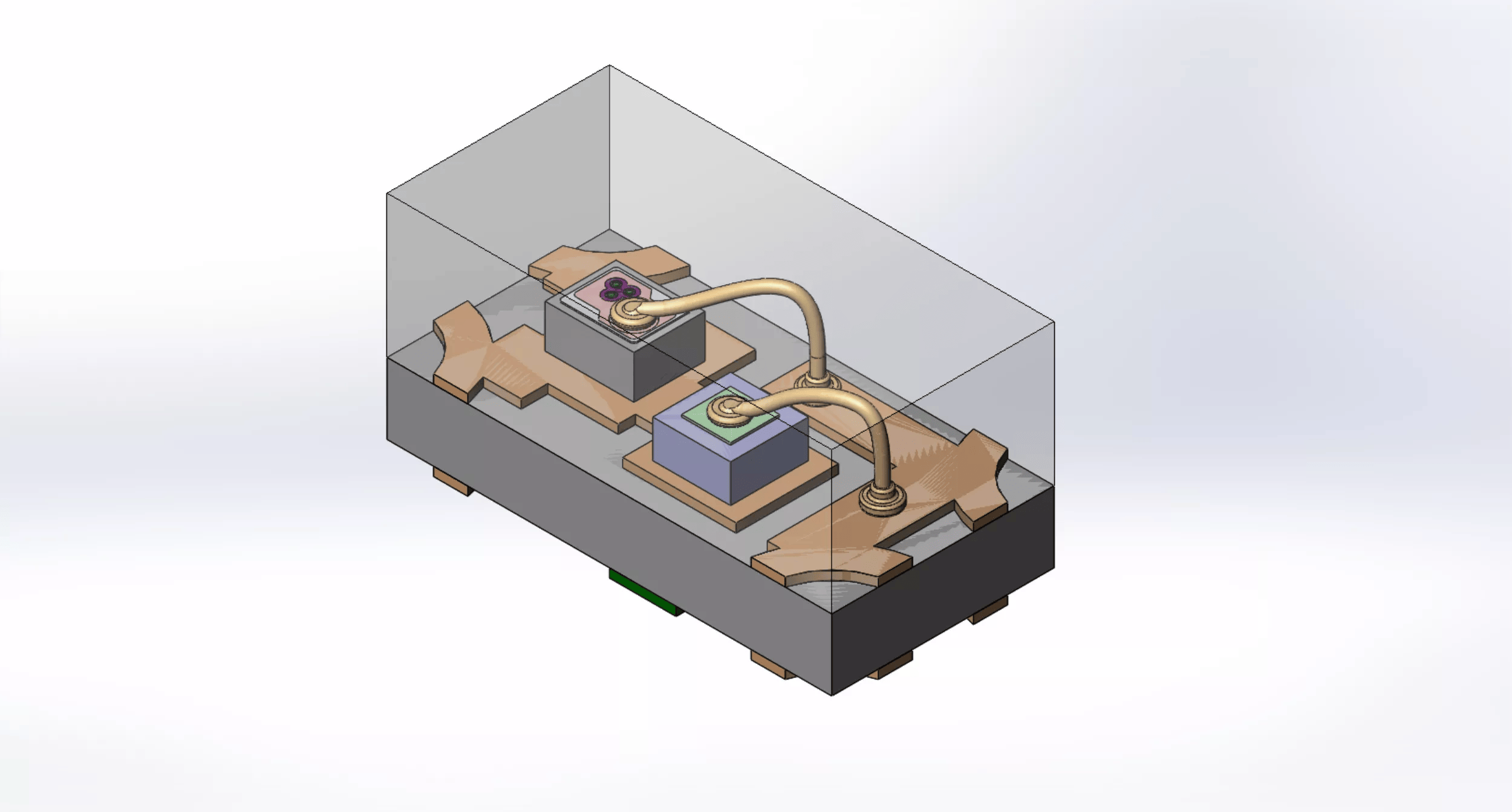 1
 1
.cob.json. Maybe this is interesting or helpful for some of you. Please let me know what you think. You should be able to try it with your own GDSII files, place PCB pads and export it to a kicad schematic + footprint. You can also use the exporter from KiCad to use the sym and fp in Altium.
Here is a writedown: https://maxclerkwell.tech/posts/open-cob-json-september-2026/
Here is the repo: https://github.com/MaxClerkwell/open.cob.json
I will add a wire-editor into my cobedit tool soonish, but so far I have figured out the wire-geometry as well as the bonding-parameters along the way.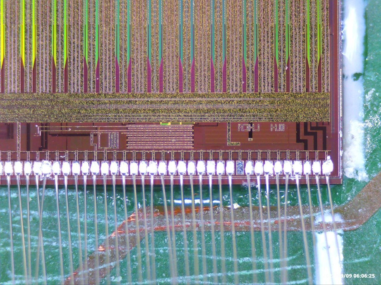 2 1
(1/e²) beam divergence is given at 18° typ 25° max and reading the intensity plot in the datasheet the full width half maximum is about 8.5°), so I could try to approximately target having an on-die photodiode good for fiber data communications with a suitable low cost VCSEL diode transmitter. Notably vague ideas of brightness and less vague ideas of beam size and spectrum matter. 2 1 1
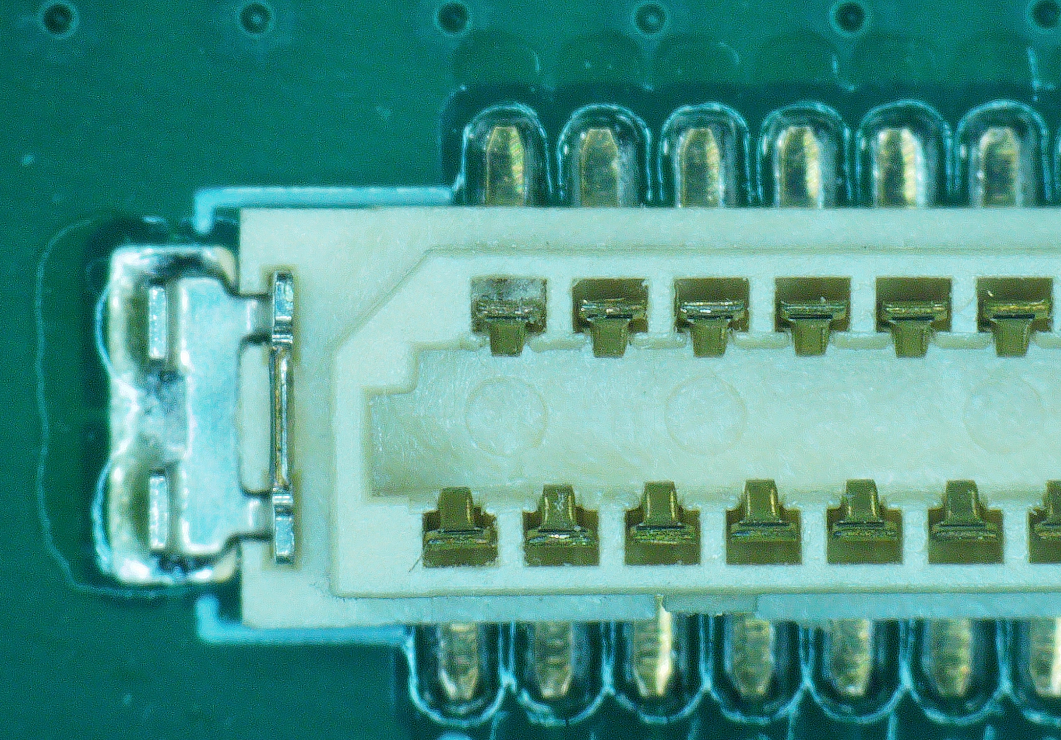 1 1 missing stuff like buried diodes and STI. should still work for a demo chip though I think
CCD would be tricky since we only have one Poly layer. But I think you could space them very close together and drive it with 3- or 4-phase clock. Probably really lossy and will bloom/smear but maybe part of the charm? 3 1 2 1 1 1
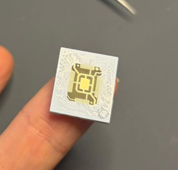
FC01 test dies.
Thickness target would be between 5 and 30 micrometers, approximately.
Surface is targeting to be attached via ACF to ENIG-plated flex-PCB, 0.33 oz 2-layer (the JLCPCB special; though this is of course negotiable but in absence of any particularly decent reason to stray from it I would favor it for being both accessible and capable of probably the finest PCB traces you can get for under 50$ shipped.FC01 test dies.
Thickness target would be between 5 and 30 micrometers, approximately.
Surface is targeting to be attached via ACF to ENIG-plated flex-PCB, 0.33 oz 2-layer (the JLCPCB special; though this is of course negotiable but in absence of any particularly decent reason to stray from it I would favor it for being both accessible and capable of probably the finest PCB traces you can get for under 50$ shipped. 
 1
 1 1
 1 1 1 2 1

 I will make a list of all requested changes for the 0.5x0.5 based on the github PR and you can ping me here if you want to request additional changes.
 1 2

FC01 die? 1