Guild icon
wafer.space Community
📐 - Designing / 📦-cob
files repo Channel for discussing chip-on-board packaging options for wafer.space bare die.
Between 2026-09-30 11:59 p.m. and 2026-11-01 12:00 a.m.

Avatar
Avatar
namibj
@Essen Hey, you did a great job I think with the attempted full die pad ring FPC fan-out; can you whip up an FPC for testing bonding the FC01 die?
Thanks, frankly I don't think I can commit to this, the next few weeks are packed. That said, I think @Stephan Bökelmann 's cobedit would be perfectly suited for this usecase. You should give it a spin.
🫶 1
Avatar
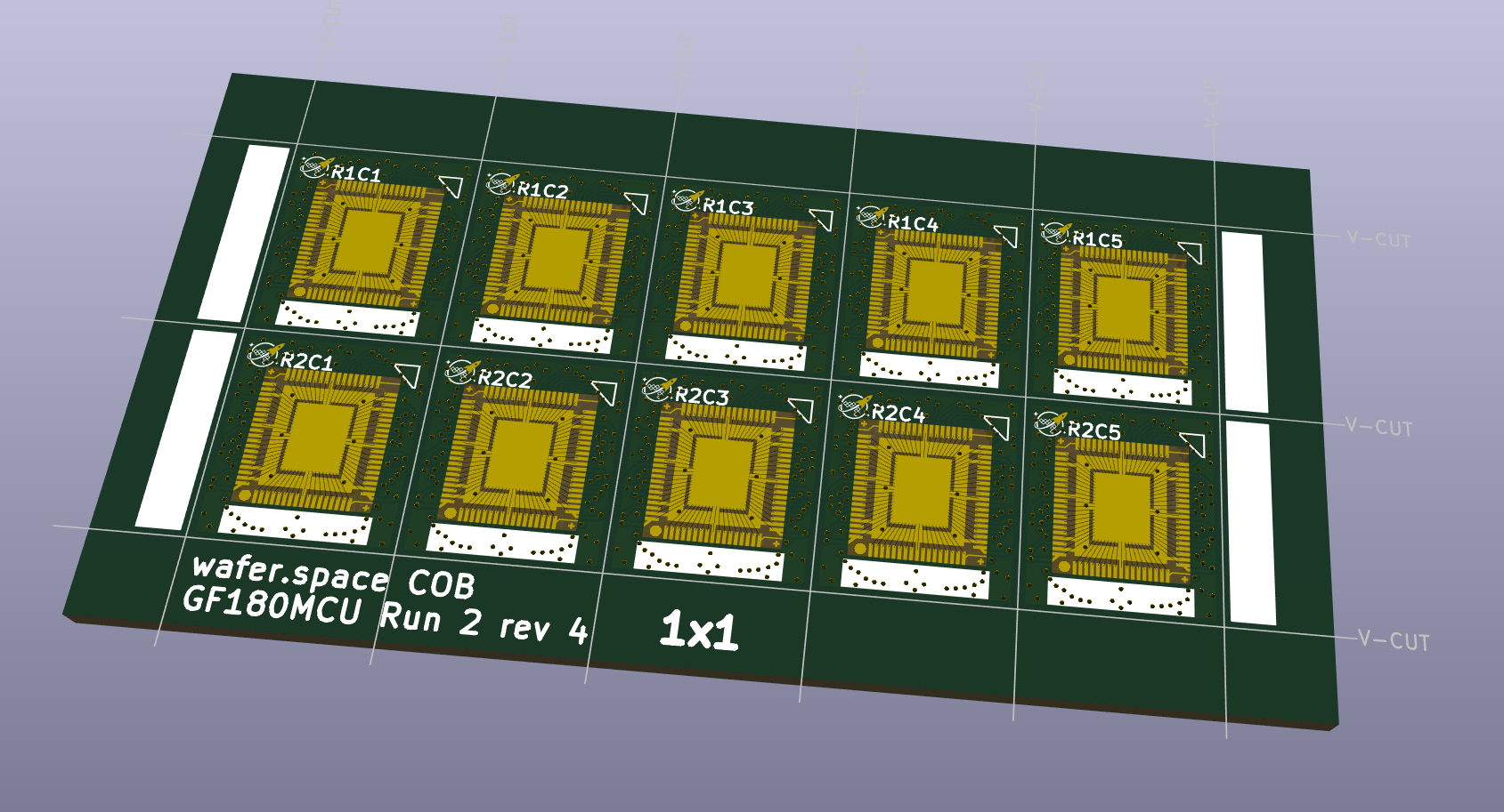
1x1 looking good!
💜 2
💯 1
Avatar
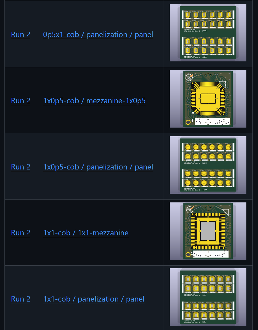
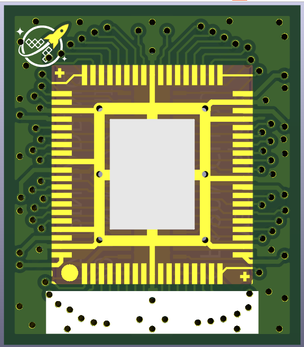
Main change is moving vias out of the region between die and pads on 1x1 and 0p5x1. Also: Enable via teardrops Add arrow marking to match die More ground fill on 1x1 And some small tweaks
❤️ 1
🔥 1
Avatar
Andrew Wingate 2026-10-05 6:56 p.m.
I'm about to leave for the airport. I'll give it a look real soon. Thank you!!
💜 2
Avatar
Andrew Wingate 2026-10-05 9:48 p.m.
Thank you @RebelMike pull request merged Currently sitting in airport, so it's difficult to concentrate, but I think they look real good. For those at home 1x1 p5x1 1xp5
💜 2
9:49 p.m.
@Tim 'mithro' Ansell if the person who made kicanvas can make it so a render of the die shows up as preview that would be really cool!!
Avatar
FWIW I think you could put all the via to have annular rings only at "Start / End / Connected" layers to reduce the cuts in the inners layers.
👍 1
Avatar
Avatar
tnt
FWIW I think you could put all the via to have annular rings only at "Start / End / Connected" layers to reduce the cuts in the inners layers.
I don't think jlc allows blind vias in their regular 4layer cheap version we're using
Avatar
That's not blind vias. They still go through and have annular ring on top and bottom .
Avatar
Andrew Wingate 2026-10-06 2:16 p.m.
ok, @stuart the panel is ready but... @Leo Moser (mole99) @tnt @Tim 'mithro' Ansell @RebelMike I think we need to talk about
  • pin1
  • what that means
  • how we want to mark it I need to get on another flight and don't really have the bandwidth at the moment to come up with a solution.
Wire bonded chip on board PCB designs. Contribute to wafer-space/chip-on-board-wire-bonded-pcbs development by creating an account on GitHub.
👍 1
2:17 p.m.
Avatar
looks like 5x2 in that image, did you change to 6x2?
2:38 p.m.
before I check the gerber files 🙂
Avatar
Andrew Wingate 2026-10-06 2:38 p.m.
-# also note @RebelMike I changed the vias per @tnt request. Thanks tnt for the suggestion.
👍 2
Avatar
Avatar
stuart
looks like 5x2 in that image, did you change to 6x2?
Andrew Wingate 2026-10-06 2:39 p.m.
it was always 5x I started with the main one and just chopped off the bottom
Avatar
Avatar
Andrew Wingate
it was always 5x I started with the main one and just chopped off the bottom
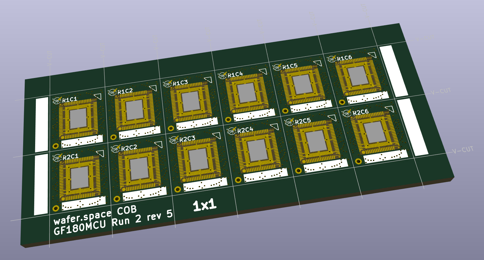
ok, can you please update to 6x2 when you have time? Maybe once we've worked out what we're doing re: the pin 1 marking?
Avatar
Avatar
stuart
ok, can you please update to 6x2 when you have time? Maybe once we've worked out what we're doing re: the pin 1 marking?
Andrew Wingate 2026-10-06 2:40 p.m.
I don't understand where this request is coming from?
Avatar
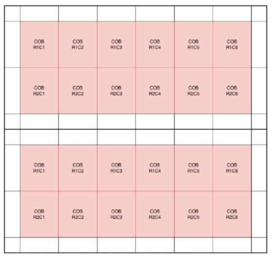
the bond house said multiples of 4 is most efficient. so 6x2 gives us 3 sets of 4
2:41 p.m.
There are a number of changes we may or may not be making for the run-2 versions. Current List: All boards 4 layers Location of the pin1 fiducial Globtop bubble fixes No vias/holes/etc. under globt...
2:42 p.m.
I don't actually see anything there about the reason for updating to 6x2, but yeah the bonding house said multiples of 4 is best
Avatar
Avatar
stuart
the bond house said multiples of 4 is most efficient. so 6x2 gives us 3 sets of 4
Andrew Wingate 2026-10-06 2:43 p.m.
so they have larger chucks than the last place?
2:43 p.m.
the factory made this drawing when giving feedback
Avatar
Andrew Wingate 2026-10-06 2:44 p.m.
ok, gotta go to bathroom and get on plane
👍 1
RebelMike started a thread. 2026-10-06 6:28 p.m.
Avatar
Andrew Wingate 2026-10-07 2:07 a.m.
Posting to main here, new panel is 6x2 and we have added a pin1 fiducial. Conversations still ongoing
Avatar
Tim 'mithro' Ansell 2026-10-07 9:30 a.m.
@stuart - Was there something from JLC about panel size or something being the cause of poor connector mounting or something? (edited)
Avatar
Avatar
Tim 'mithro' Ansell
@stuart - Was there something from JLC about panel size or something being the cause of poor connector mounting or something? (edited)
I don't think so
Avatar
Avatar
Tim 'mithro' Ansell
@stuart - Was there something from JLC about panel size or something being the cause of poor connector mounting or something? (edited)
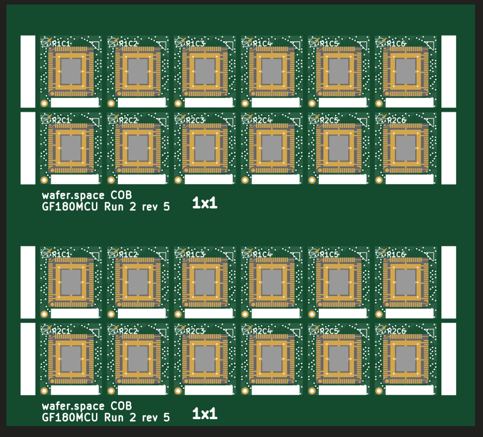
Turns out you were right about this - after checking for quotation on JLC, the panels are now too small. @Andrew Wingate apologies but can you please double them up - so we have (6x2)x2 - so two bonding panels per PCBA panel? Like this. This should avoid any additional cost. My bad for not realising this earlier 🙂
👀 1
Avatar
Andrew Wingate 2026-10-08 2:58 p.m.
Ok, I've panelized the half slots and have merged @RebelMike pull requests. Thank you again I'll look at the p5xp5 tomorrow
💜 2
❤️ 1
Avatar
@Andrew Wingate Not sure how we missed this, but there shouldn’t be soldermask between the die and the pins on the quarter slot
Avatar
Avatar
RebelMike
@Andrew Wingate Not sure how we missed this, but there shouldn’t be soldermask between the die and the pins on the quarter slot
Andrew Wingate 2026-10-09 7:06 a.m.
Oof good catch. I'll fix right now, will be a bit before i have internet again
Avatar
Thanks!
Avatar
Avatar
RebelMike
Thanks!
Andrew Wingate 2026-10-09 9:09 a.m.
Fixed p5xp5 and pushed. Good catch and thanks @stuart I went back and double checked them all as a second pass. Seemed the v-cut checkbox was turned off on the p5x1, might be good to regrab them all
👍 1
Avatar
regrabbing now then will place orders
💯 1
Avatar
@Andrew Wingate I just noticed that the 0p5x0p5, 0p5x1 and 1x0p5 BOMs don't have a defined capacitor value. Should they be 1uFs, the same as for the 1x1s? Also for all BOMs is it worth adding the LCSC part number, C19089236?
Avatar
Avatar
stuart
@Andrew Wingate I just noticed that the 0p5x0p5, 0p5x1 and 1x0p5 BOMs don't have a defined capacitor value. Should they be 1uFs, the same as for the 1x1s? Also for all BOMs is it worth adding the LCSC part number, C19089236?
Sorry missed that. Yes, 1uF would be great for them all
👍 1
Avatar
Avatar
stuart
Turns out you were right about this - after checking for quotation on JLC, the panels are now too small. @Andrew Wingate apologies but can you please double them up - so we have (6x2)x2 - so two bonding panels per PCBA panel? Like this. This should avoid any additional cost. My bad for not realising this earlier 🙂
Tim 'mithro' Ansell 2026-10-09 9:33 p.m.
I think the complaint from JLC PCB was about the PCBs being quite thin and warping slightly during the PCBA process causing bad connector adhesion? Do you know if there are any reasons we use such thin PCB?
Avatar
Avatar
Andrew Wingate
Sorry missed that. Yes, 1uF would be great for them all
Tim 'mithro' Ansell 2026-10-09 9:36 p.m.
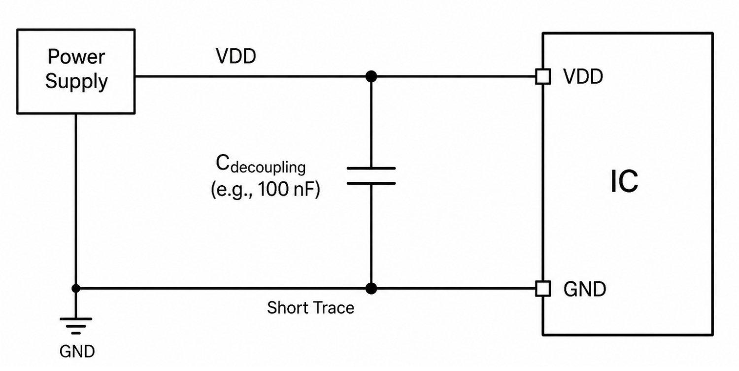
I'm pretty sure that for things like this the actual capacitance doesn't matter hugely, but the capacitor response/type does? https://jlcpcb.com/blog/decoupling-capacitors-guide
Master decoupling capacitor placement, values, and layout guidelines to eliminate voltage droop, EMI, and noise in your high-speed PCB designs.
Avatar
Avatar
Tim 'mithro' Ansell
I think the complaint from JLC PCB was about the PCBs being quite thin and warping slightly during the PCBA process causing bad connector adhesion? Do you know if there are any reasons we use such thin PCB?
reason for the thin PCB afaik is because you asked for it 😉 I would be happy to go for thicker in the future if there's no reason not to? (edited)
Avatar
Andrew Wingate 2026-10-10 6:34 a.m.
@stuart re: jlc issue. Currently moving about I'll take a closer look when i get settled somewhere
Avatar
Andrew Wingate 2026-10-10 6:46 a.m.
Also @stuart can you let me know which board that is. I'll likely just change things to adhere to their specs and give you a new file
👍 1
Avatar
Avatar
Andrew Wingate
Also @stuart can you let me know which board that is. I'll likely just change things to adhere to their specs and give you a new file
It's the 1x1, all the rest seem to be ok
👍 1
Avatar
@stuart panels are ready and new files exported.
Wire bonded chip on board PCB designs. Contribute to wafer-space/chip-on-board-wire-bonded-pcbs development by creating an account on GitHub.
❤️ 2
Avatar
Avatar
Tim 'mithro' Ansell
I'm pretty sure that for things like this the actual capacitance doesn't matter hugely, but the capacitor response/type does? https://jlcpcb.com/blog/decoupling-capacitors-guide
The reason for the thinner PCBs was an attempt to reduce wire lengths, and was also suggested by @tnt if memory serves. I think it would be alright to go to 1.0mm or even 1.2mm if we're having problems. 1.6mm would be too chunky for the size of these boards.
12:27 p.m.
Also the length from the die to the pcb is probably the most determining factor [for decoupling performance]. And having them on the PCB itself gets it as close as possible (edited)
Avatar
For decoupling 100n is a very outdated value. 1u is definitely a good pick here. But yeah, the trace length and width ( in general the inductance ) will be a big factor for the performance. GF180 drivers have pretty fast edges and I was seeing a lot of ringing and ground bounces on the TT dies from run 1.
💜 1
👍 1
Avatar
Avatar
tnt
For decoupling 100n is a very outdated value. 1u is definitely a good pick here. But yeah, the trace length and width ( in general the inductance ) will be a big factor for the performance. GF180 drivers have pretty fast edges and I was seeing a lot of ringing and ground bounces on the TT dies from run 1.
We have been using 1uF
👌 2
Avatar
Avatar
Andrew Wingate
@stuart panels are ready and new files exported.
Thanks, re-order placed
💜 1
🎉 2
Avatar
Avatar
stuart
reason for the thin PCB afaik is because you asked for it 😉 I would be happy to go for thicker in the future if there's no reason not to? (edited)
Tim 'mithro' Ansell 2026-10-10 10:46 p.m.
@Andrew Wingate - Did the thin PCB come from you?
10:47 p.m.
@Andrew Wingate - Oh, you already replied above.
👍 1
Exported 51 message(s)
Timezone: UTC+0