Hey everyone, like Tim mentioned, we’re building a die-sorting robot!
To give you a sense of scale, here’s what one run looks like:
50 full wafers
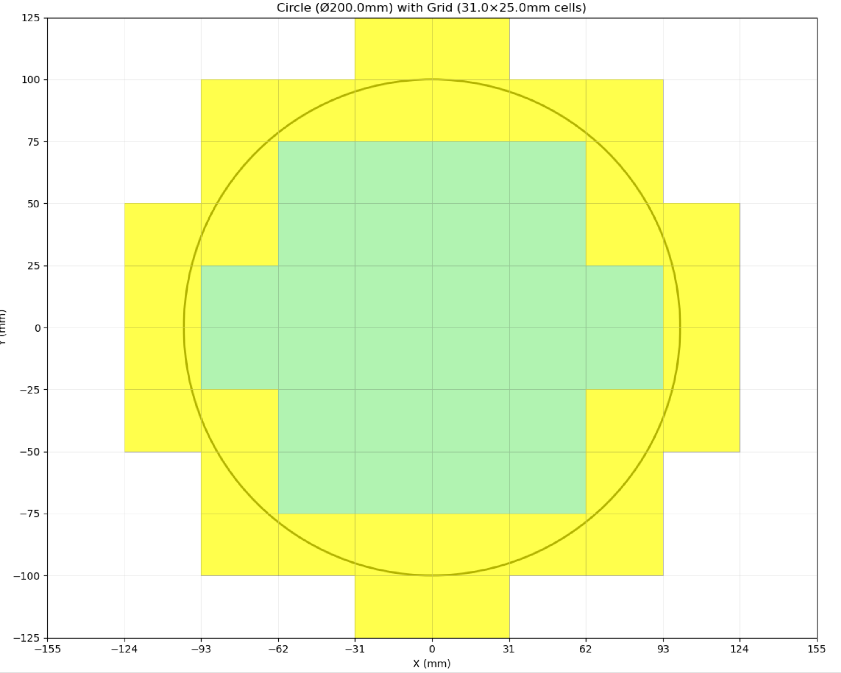
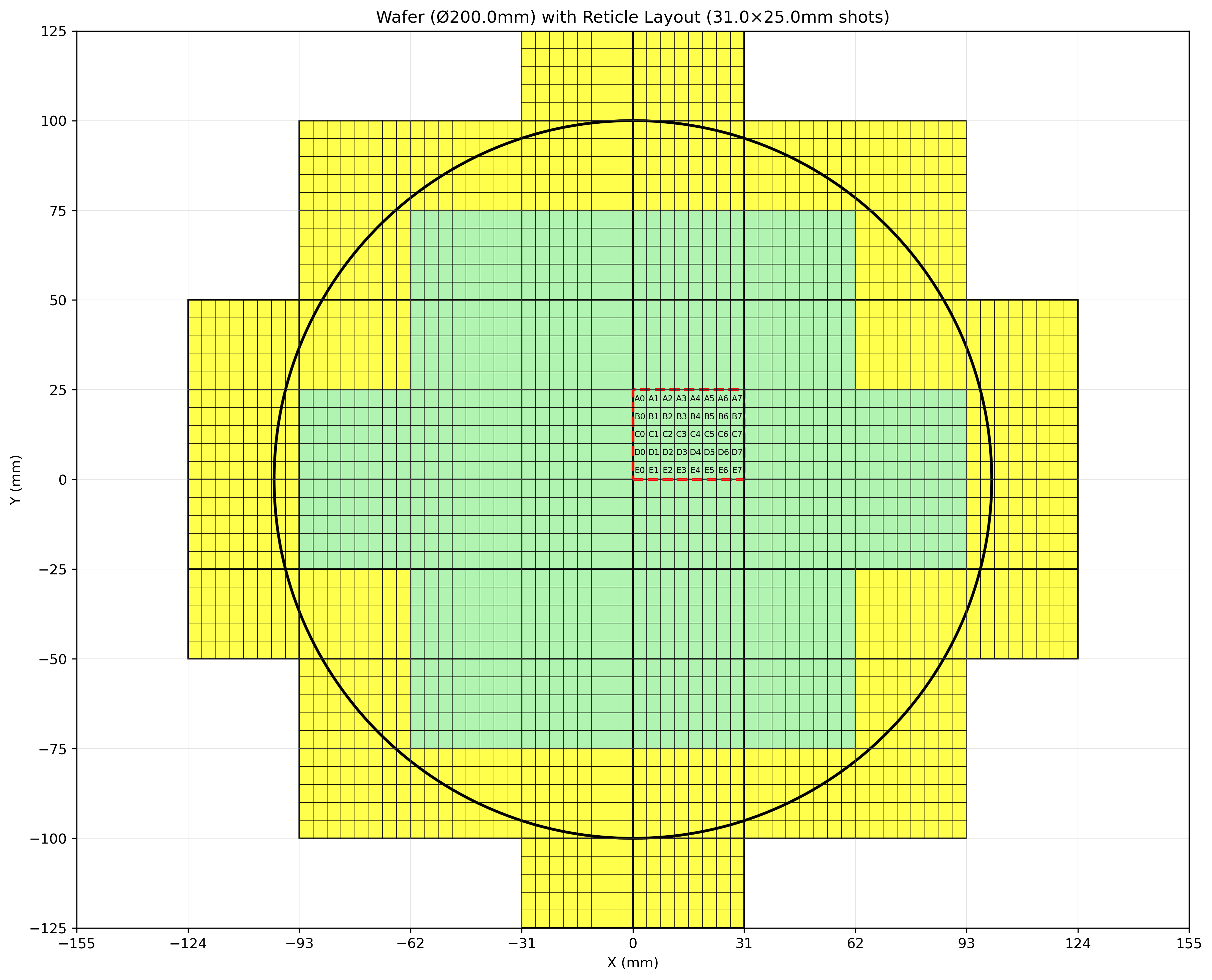
28 reticle shots (each a “group photo” of all projects) per wafer
40 unique projects per reticle shot
Add it up and you get 56,000 project dies
Each die is about the size of a few grains of rice: 3.88 mm × 5.08 mm
Laid out flat, that’s over 8 ft² (0.8 m²) of silicon — basically a coffee table made of chips
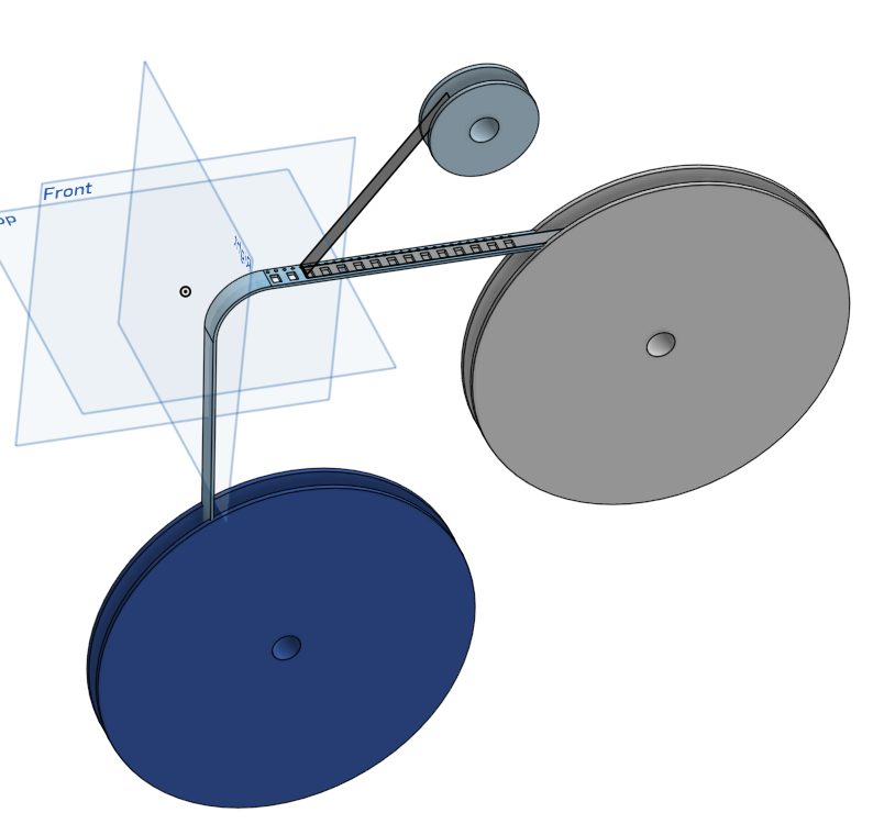
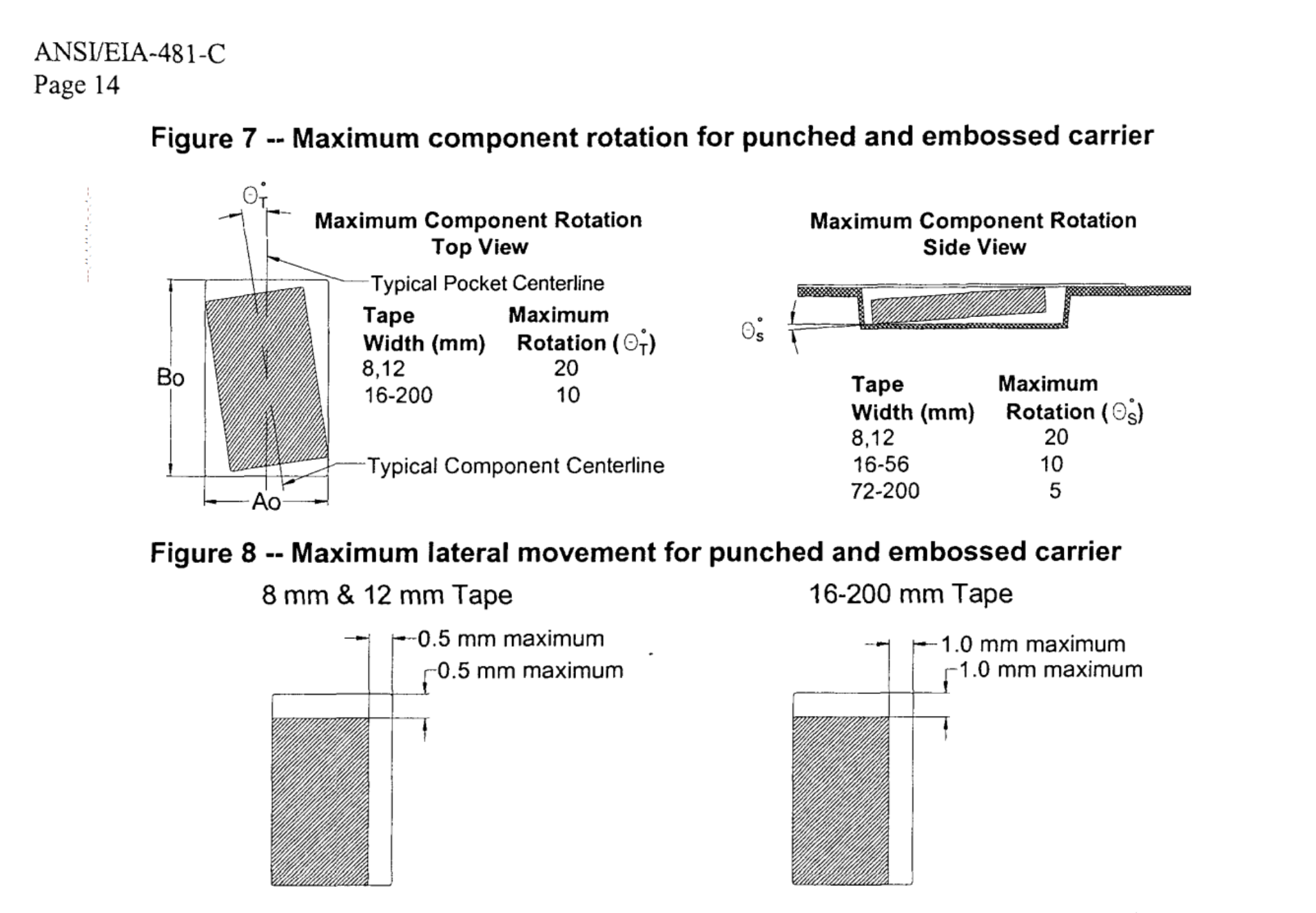
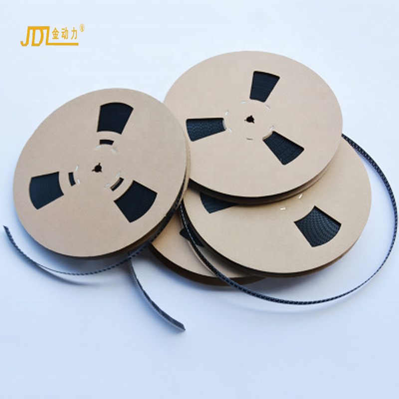
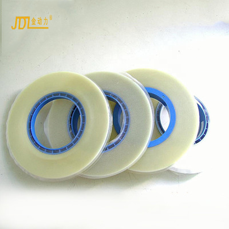
In electronics manufacturing, tape-and-reel is the standard way to package components, so that’s our target. We looked at wafer packs (think plastic ice cube trays for chips) and gel packs, but reels make the most sense at this scale.
The wafers will arrive pre-sliced and mounted on tape frames. With so many dies to handle, we’re going straight from wafer to reel — no detours.
I can’t wait to see all the designs people come up with, and I’ll keep posting updates as this project rolls forward (pun intended).
Yeah.. it's kinda close in sq units. it's a thumbnail at 1mm
2:21 a.m.
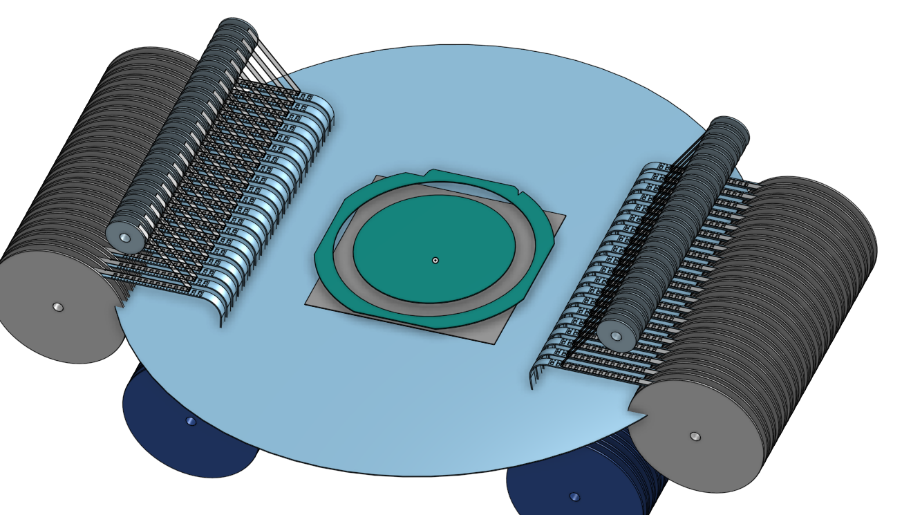
These are very early models, just exploring how all the pieces might fit together into a compact machine; after all, this whole setup has to ship to Singapore!
The concept is straightforward: the wafer sits right in the center, surrounded by 40 tape-and-reel stations (20 on each side). Each station will load a specific die into its own reel and then seal it up with protective film, ready for shipping :)
Thx for some of the info Tim, -edit for those watching, we're looking to put dies into smt tape
EIA STANDARD - 8 mm Through 200 mm Embossed Carrier Taping and 8 mm & 12 mm Punched Carrier Taping of Surface Mount Components for Automatic Handling(edited)
The process, packaging, and materials cannot impact the components. This includes their markings and their electrical and mechanical characteristics. Additional guidelines exist for further reference, including:
EIA-383—Preparation for the Delivery of Electrical and Electronic Components
EIA-541—Packaging Material Standards for ESD Sensitive Items
EIA-583—Packaging Material Standards for Moisture Sensitive Items
EIA-624—Product Package Bar Code Label Standard for Non-Retail Applications
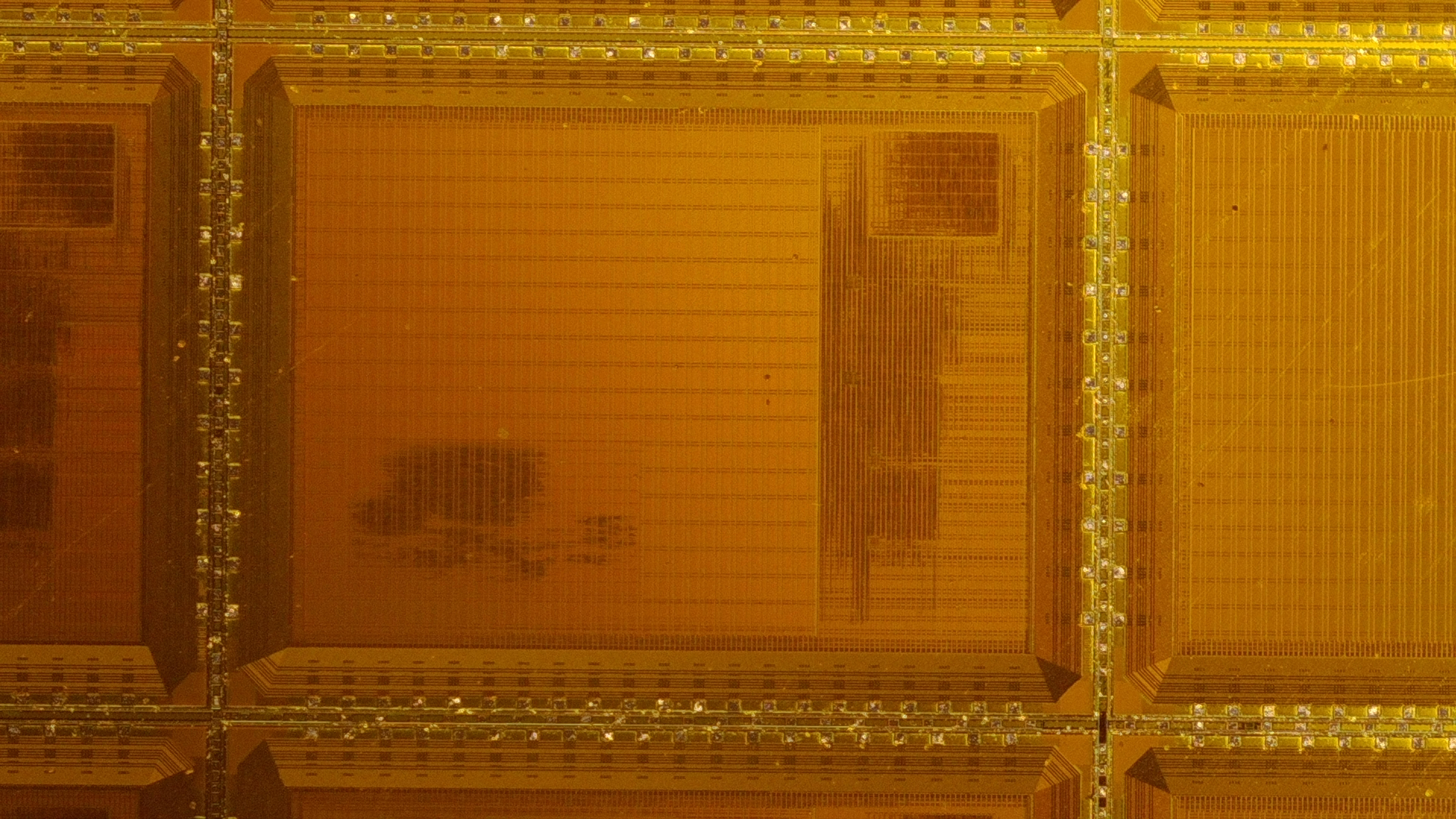
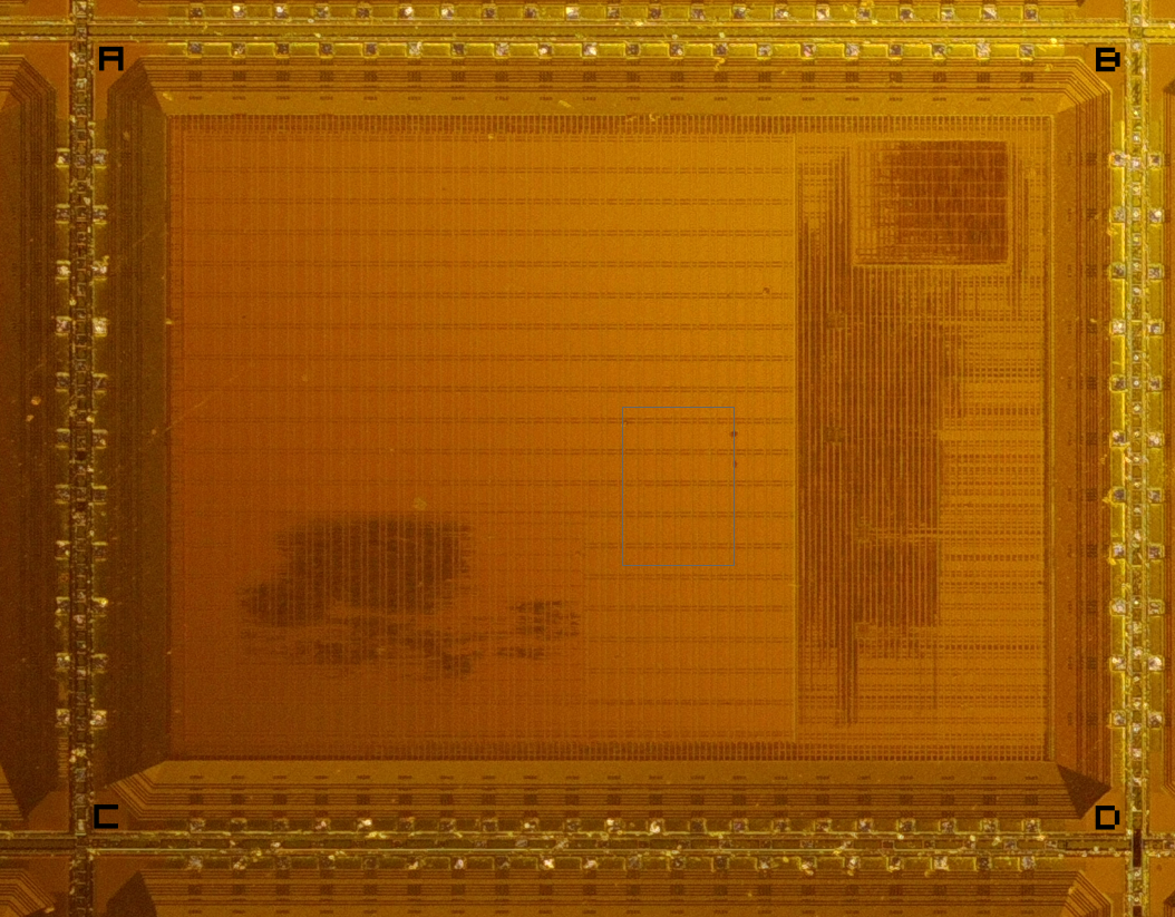
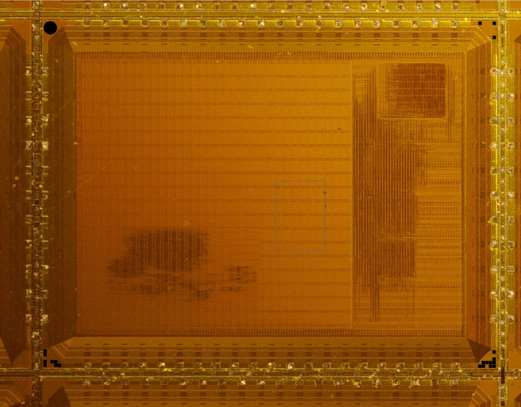
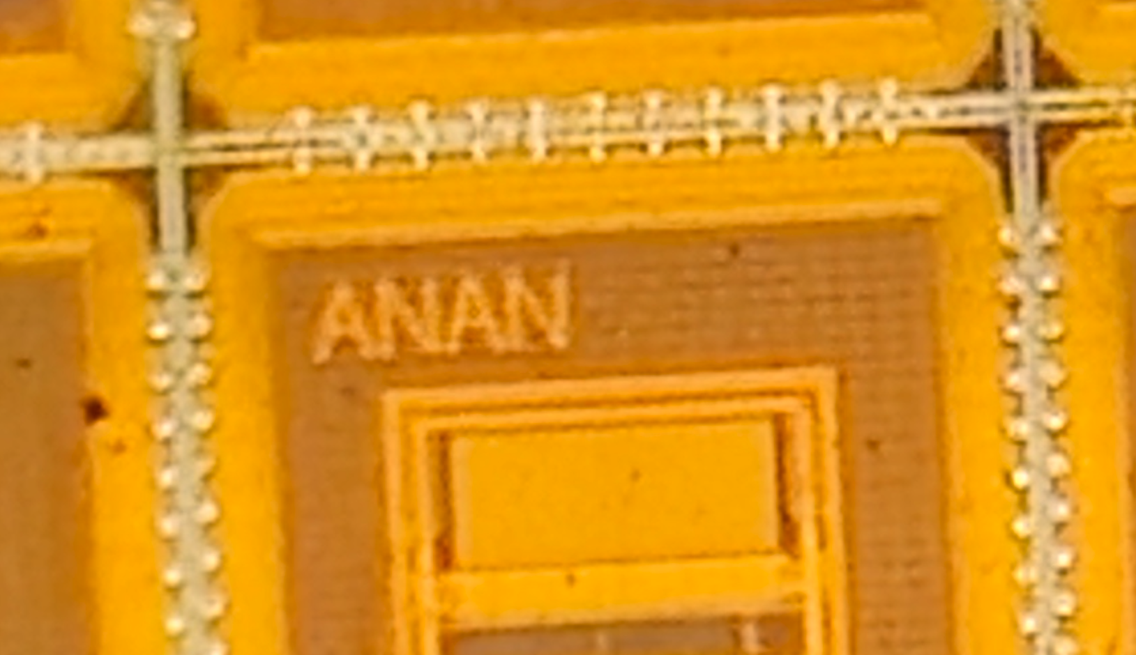
@Tim 'mithro' Ansell I've been playing with a few cameras and microscopes that I have. That 2mp camera I was talking about cannot read these IDs. Also the crappy usb microscope I have also does nothing to help.
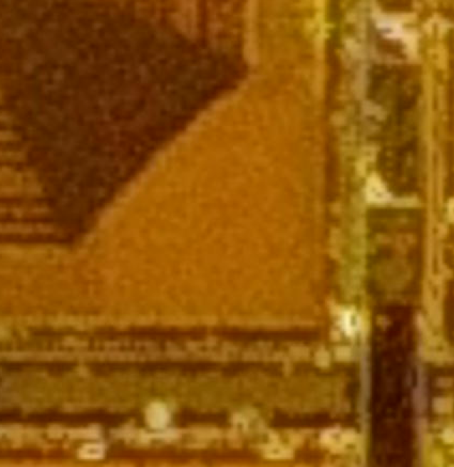
I also have a 48MP microscope and it also cannot read these id's. What I have shown here is about the best zoom I'm able to get out of it. It's possible with some better light we could get a better look, but at the end of the day these are very very small features.
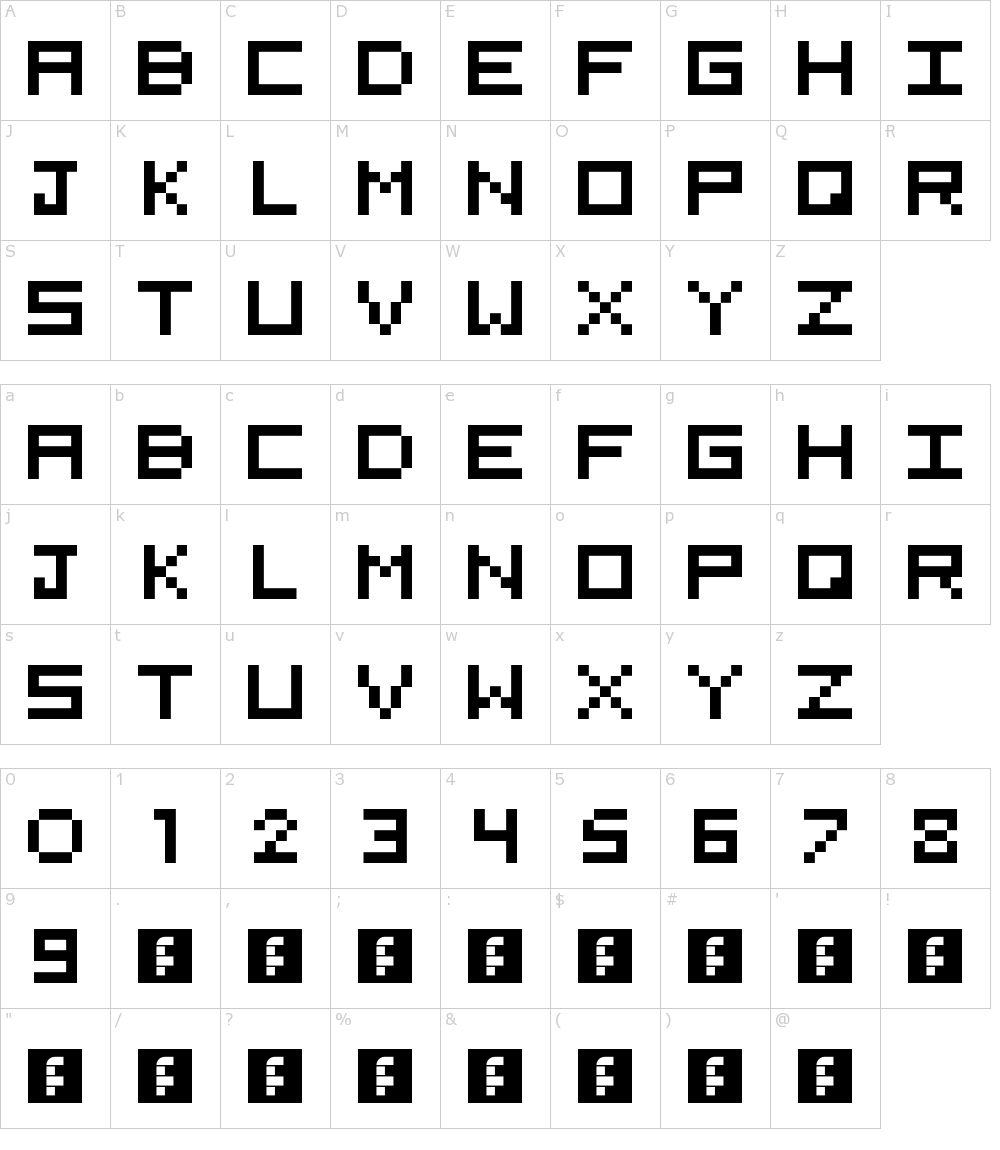
I came up with this and wanted your opinion of if this is a viable option.
The idea is to create larger characters that can fit in every corner. The process and run could somehow be encoded if desired, but all that info is in the id anyways.
tnt
I would have tought you'd use the position on the wafer to sort, not trying to read those tiny IDs.
Tim has expressed interest in verification steps along the way.
Additionally, there seems to be little trust that all wafers will be the exact same (even if this is just how things are mounted on the wafer frame after dicing.
so I'd just keep it as simple as possible.
Maybe like 2x2 matrices on each edge, that gives you a total of 16 bits, so you could actually encode the data twice + parity? You can also use some of the bits for detecting the orientation
9:37 a.m.
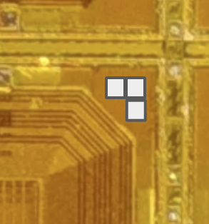
Looking at the space, triangle shape (3-bits) will probably fit better
urish
so I'd just keep it as simple as possible.
Maybe like 2x2 matrices on each edge, that gives you a total of 16 bits, so you could actually encode the data twice + parity? You can also use some of the bits for detecting the orientation
BTW, are raw dies on reel something common ? (i.e. would packaging house usually be equipped to handle that)
5:05 p.m.
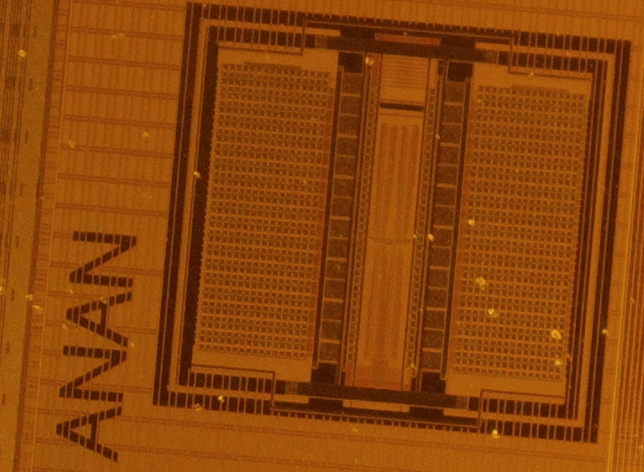
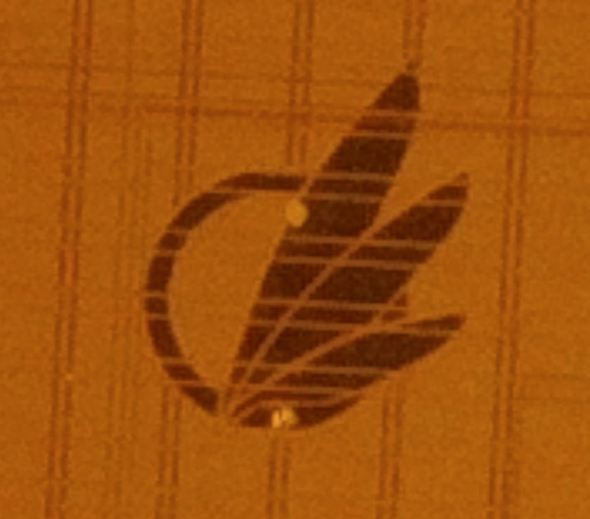
Side note: I tried reading the die-ID on my MPW1 chip with my microscope and no way ... I can barely make-out the OSHW logo and that's if I light it at just the right angle ...(edited)
At the moment the IDs which where used on the Google shuttles don't seem to be easily readable by the equipment that @tnt or @Andrew Wingate have. Thus it might be good for us to go with an ID which is bigger and allows more people to read them easily without having to get a good microscope from you
1
tnt
Yeah, because of pick and place machines, but if the machine dealing with dies aren't made for those, that won't help
@tnt - Yeah, these are the type of questions we are trying to sort out now, I'd like to do at least some type of short PCBA with wire bonding run (probably using GFMPW-0 or GFMPW-1 ICs) ASAP.
Tim 'mithro' Ansell
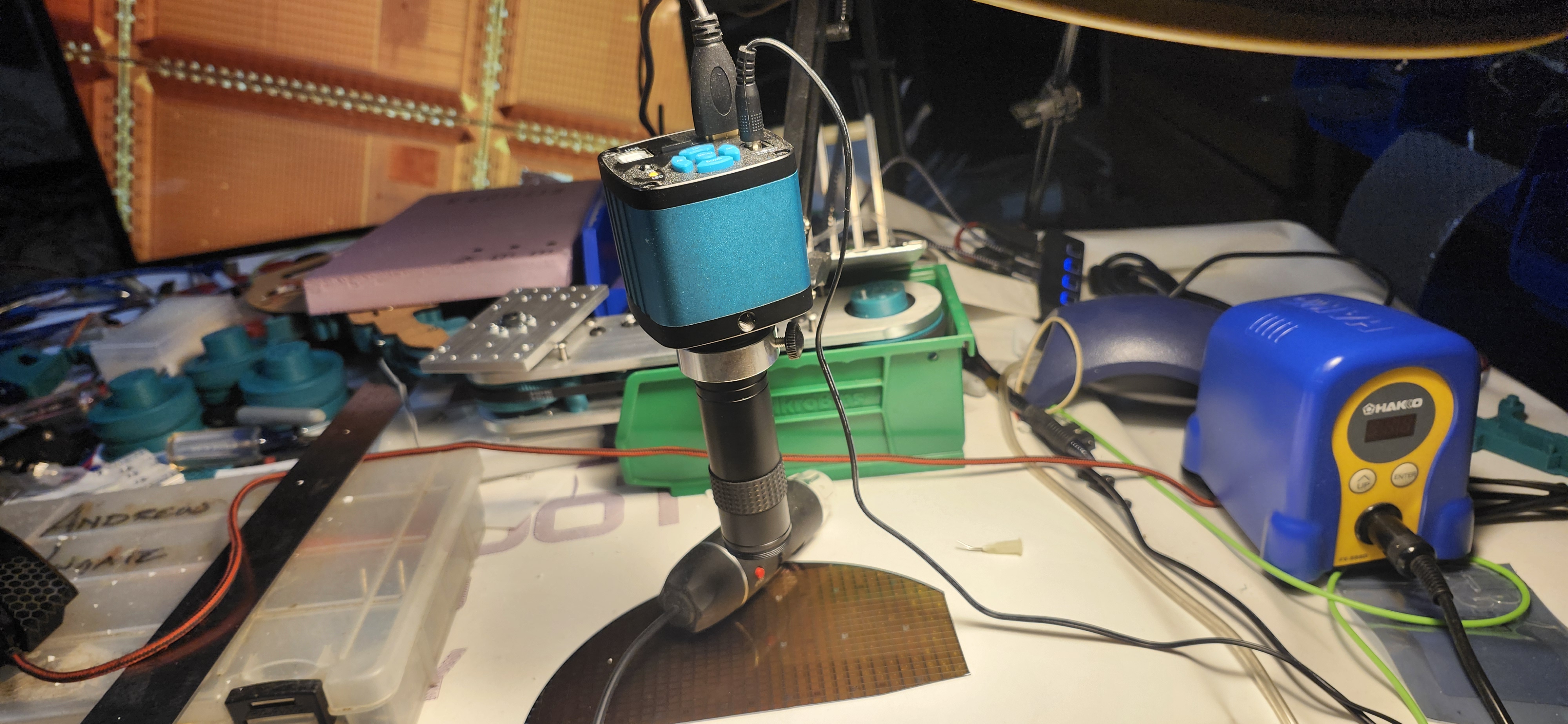
@Andrew Wingate - Do you have pictures of your microscope / camera set up?
Pardon the mess.
This is the microscope I used to send the picture above. The crappy little black usb microscope on it's side also did not seem to work very well. Some of it could be bad lighting, user error, or they really are just too small to be read by crappy equipment.
1
Tim 'mithro' Ansell
@Andrew Wingate / @Leo Moser (mole99) - We probably want a "pin 1" type marker as well for orientation.
I was trying to come up with something that would still be at least partially useful if the dies were cut up further, but I think now that's another problem.
Expanding on @urish idea of some bitwise information encoded into the corners we could also go maybe as far as something like this
if the corners of the triangles are always black--or whatever color--that could be used to identify location/skew/etc. and if triangle has a side length of 5 that leaves 12bits of info per corner--this obviously does not count for the pin1 corner though.
The deeper we dive into this, the more it seems like it may be useful to keep these human readable.
Oh, of course!
I was just throwing anything at the wall to see if it sticks.
You are correct, I've been thinking more application than implementation.
@Leo Moser (mole99) I would love some advice on what's possible and easiest to implement.
2:29 a.m.
@Leo Moser (mole99) I see on this chip I have there are ?different layers? that have different colors. Is it possible to do something like what's pictured here for the best contrast?
2:32 a.m.
It seems there are a couple dies on this wafer that have done something similar
I'm on my way back from Austrochip, so I can reply to questions again :)
I started gf180mcu-precheck a few days ago. It is a custom LibreLane flow to read the user GDS, perform various checks (e.g. top-level, density, etc.), insert the ID, and whatever else we need. At the end, you receive the final GDS used for fabrication.
I use the KLayout API to generate the shapes for the ID. Currently, I'm using the built-in TEXT PCell to generate the digits for the ID, but we can use anything else: a QR code, a pattern of dots etc.
One thing to consider: we should not specify a fixed position for the ID. Instead, we provide an abstract cell for the ID that the user can place anywhere on their die, which is later replaced with the generated ID. This allows to do custom padframes (or no padframes at all). I can extract the position of the ID cell during the precheck. With the location of the die on the reticle and the offset of the ID, you can position the camera above the ID.
As for the layers, I would place the ID at Metal5 (topmost layer) with a no-fill shape around it. I assume this will give enough contrast. There are ways to achieve different colors with diffraction patterns, however, I'm no expert on that :)
Hey @mole99, I figured this was the best place to continue this conversation about the ID location, design, and layer. You posted: One thing to consider: we should not specify a fixed position for ...
4:05 a.m.
I would love people like @tnt to be able to identify they got the right part and the pin zero / orientation
@Tim 'mithro' Ansell and @Leo Moser (mole99)
For reference, the first pic was taken with my phone. Pretty new samsung.
Second is taken with one of those super cheap usb microscopes
Andrew Wingate
@Tim 'mithro' Ansell and @Leo Moser (mole99)
For reference, the first pic was taken with my phone. Pretty new samsung.
Second is taken with one of those super cheap usb microscopes