
wafer.space Community
Information / general
Welcome to wafer.space - documentation at wafer.space github - buy at buy.wafer.space - archives at discord.wafer.space
Between 2025-09-30 11:59 p.m. and 2025-11-01 12:00 a.m.

 1
1


 1
1
 1 1
1 1 Hacker News • 2025-10-02 10:12 p.m. 1 1


 1 2 1 1 2
")

 1
1 maybe I should try that PDK crowdsupply.com/wafer-space/gf…
Upside: you get to do your own padring!
Downside: you have to do your own padring! (and ESD)
maybe I should try that PDK crowdsupply.com/wafer-space/gf…
Upside: you get to do your own padring!
Downside: you have to do your own padring! (and ESD) types.pl • 2025-09-26 12:18 a.m.
  1 1
1 1
 1 1 1 1
 3 3
3 3
 1
1gf180mcu/gf180mcuD/libs.tech/klayout/tech/drc/filler_generation/: tile_size is defined individually in each script, and $threads is defined in fill_all.rb. ♂️
♂️
nix-shell starts building stuff from source.nix-shell. This is because we're currently using a branch of LibreLane and therefore not all binaries are cached. This will improve once most of the changes have been upstreamed.") 3
3 1
1
 4
4 2
2 1
1


 1 8
1 8  1 2 1 1 2
") 1
1")
") 1
1 1
1 1
1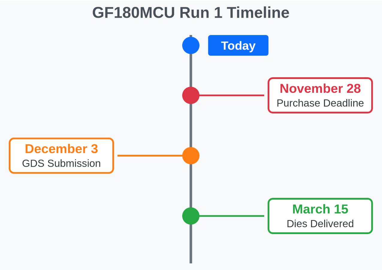 2 2 2
2 2 2 1 4
1 4
")
")
")
")

