
wafer.space Community
Information / general
Welcome to wafer.space - documentation at wafer.space github - buy at buy.wafer.space - archives at discord.wafer.space
Between 2026-03-31 11:59 p.m. and 2026-05-01 12:00 a.m.


")


 5
5

 1
1


 2
2 1
1 Hacker News • 2026-04-05 5:50 a.m.


|s, it's router1, if it has =s, it's router2--router router2synth_aegis command would be cool, it would only really need the JSON descriptor I think. 1 try to follow whenever a good project pops up!
 1
1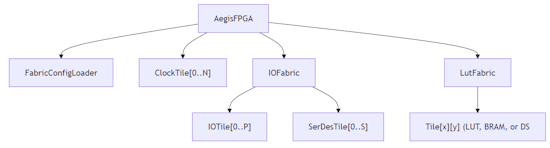
 1
1DRT_THREADS set to the number of machine threads, and many other parts of the flow are single-threaded.-threads $NIX_BUILD_CORES 1
 3 1 1 1
 1 1 1 2
 1
1 1
1


 1
1 2
2") 1
1 1
1


 Finally, I had everything I needed to do the bring-up of the chip.
I was a bit surprised when it just... worked!
Greyhound is an open-source RISC-V SoC with tightly coupled eFPGA. The chip was designed using LibreLane (https://librelane.org/) and FABulous (https://lnkd.in/gkhEg66j), and the FPGA toolchain uses Yosys an... 6
Finally, I had everything I needed to do the bring-up of the chip.
I was a bit surprised when it just... worked!
Greyhound is an open-source RISC-V SoC with tightly coupled eFPGA. The chip was designed using LibreLane (https://librelane.org/) and FABulous (https://lnkd.in/gkhEg66j), and the FPGA toolchain uses Yosys an... 6
ERROR add_global_connections failed to make any connections for 'rst_n_pad/DVDD' to VDD. (edited) 1
 2
2")

 2
2
box mode and a few time the wiring mode. Never use import from spice or the other mode .....

 i'll do at least a few, the cross-sections I did of a i486 were a huge hit on the channel a few years ago (ditto to ion etching xsections)
")
")

 All that hard work has paid off when you finally hold the chips in your hands ✨
")
")
") 8
8 It’s so exciting to see the actual dies. Thanks everyone at wafer.space and everyone involved for making that possible
  https://github.com/meiniKi/gf180mcu-fazyrv-hachure
Shuttle ID: G801
Code: CAFE
Can’t wait to make some more close up photos under a better microscope and bring up the chip
https://github.com/meiniKi/gf180mcu-fazyrv-hachure
Shuttle ID: G801
Code: CAFE
Can’t wait to make some more close up photos under a better microscope and bring up the chip  (edited)
") 1 2 It’s so exciting to see the actual dies. Thanks everyone at wafer.space and everyone involved for making that possible
https://github.com/meiniKi/gf180mcu-fazyrv-hachure
Shuttle ID: G801
Code: CAFE
Can’t wait to make some more close up photos under a better microscope and bring up the chip (edited)
1 2 It’s so exciting to see the actual dies. Thanks everyone at wafer.space and everyone involved for making that possible
https://github.com/meiniKi/gf180mcu-fazyrv-hachure
Shuttle ID: G801
Code: CAFE
Can’t wait to make some more close up photos under a better microscope and bring up the chip (edited)  3 1
3 1 Such a good feeling. Thanks again!
")
")

") 1 1
1 1
") 1 1
1 1 )..), so.... yeah.
Good chances thus for the MCML I'm hoping to get done by the ttsky26a deadline to be easily portable to WS Run2, with mostly scripted tuning to the quite different process, but somewhat manual adaption to the different stackup.
)..), so.... yeah.
Good chances thus for the MCML I'm hoping to get done by the ttsky26a deadline to be easily portable to WS Run2, with mostly scripted tuning to the quite different process, but somewhat manual adaption to the different stackup.") )..), so.... yeah.
Good chances thus for the MCML I'm hoping to get done by the ttsky26a deadline to be easily portable to WS Run2, with mostly scripted tuning to the quite different process, but somewhat manual adaption to the different stackup. 1
)..), so.... yeah.
Good chances thus for the MCML I'm hoping to get done by the ttsky26a deadline to be easily portable to WS Run2, with mostly scripted tuning to the quite different process, but somewhat manual adaption to the different stackup. 1 )..), so.... yeah.
Good chances thus for the MCML I'm hoping to get done by the ttsky26a deadline to be easily portable to WS Run2, with mostly scripted tuning to the quite different process, but somewhat manual adaption to the different stackup. 1 1 1
)..), so.... yeah.
Good chances thus for the MCML I'm hoping to get done by the ttsky26a deadline to be easily portable to WS Run2, with mostly scripted tuning to the quite different process, but somewhat manual adaption to the different stackup. 1 1 1 )..), so.... yeah.
Good chances thus for the MCML I'm hoping to get done by the ttsky26a deadline to be easily portable to WS Run2, with mostly scripted tuning to the quite different process, but somewhat manual adaption to the different stackup.
)..), so.... yeah.
Good chances thus for the MCML I'm hoping to get done by the ttsky26a deadline to be easily portable to WS Run2, with mostly scripted tuning to the quite different process, but somewhat manual adaption to the different stackup. ")
")
poly.2 about min spacing was fixable by just adding a few poly boxes; the otheres are basically via pushing though, I don't do that by hand.
There definitely is optimization work that differentiates through spice though.nix ps shows the klayout command has been running for 9017.5s 1
1
")
")
")
")
") 7
7 2
2via.5a: via.5a : min. m1 enclosure of 0.15um via of 2 adjacent edges : 0.085um aren't as easy because e.g. that one seems to only blame the via's perimeter for that rule violation, despite it actually being the surrounding geometry on m1 that is too close. Sure, if the via wasn't minimum size it could be shrunk and if m1 would suffice then it would then resolve.
But yeah, needs better attribution of blame to the actual vertices that are too close.
@Leo Moser (mole99) your/ @Clyde Laforge 's work on the KLayout DRC refactor, does that touch the concept of attributing DRC violations to ALL the responsible source vertices, or is it orthogonal to introduction of such a concept?via.5a: via.5a : min. m1 enclosure of 0.15um via of 2 adjacent edges : 0.085um aren't as easy because e.g. that one seems to only blame the via's perimeter for that rule violation, despite it actually being the surrounding geometry on m1 that is too close. Sure, if the via wasn't minimum size it could be shrunk and if m1 would suffice then it would then resolve.
But yeah, needs better attribution of blame to the actual vertices that are too close.
@Leo Moser (mole99) your/ @Clyde Laforge 's work on the KLayout DRC refactor, does that touch the concept of attributing DRC violations to ALL the responsible source vertices, or is it orthogonal to introduction of such a concept? 
via.5a with KLayout though as that just blames the edges of the via not mentioning the metal to put/extend there.
Does work for e.g. m2.2 : min. m2 spacing : 0.14um though, at least the ones that are min-distance-between-EdgePair's. ♂️ Should be able to get some nicer stitches once we get one. Ditto to a polarizer that fits my macro camera lens. Hoping to do some de-layering but not holding my breath that I'll get usable results from that
")
")
")
")
")
") 1 4 2
1 4 2 1♂️ Should be able to get some nicer stitches once we get one. Ditto to a polarizer that fits my macro camera lens. Hoping to do some de-layering but not holding my breath that I'll get usable results from that hopefully a light lapping of the top layer will remove all the fill and help show more details hopefully a light lapping of the top layer will remove all the fill and help show more details 4
We have a surface plate at work that generally gets abused for sanding/lapping so I'm thinking to grab that + some fine diamond paper? Trying to figure out the best way to fixture it to prevent rounding/tilt though. I dont have a tripod fixture, although I guess I could DIY without much hassle? Maybe just glue 3-4 chips onto a flat piece of metal and hope it's fairly planar across all of them
1♂️ Should be able to get some nicer stitches once we get one. Ditto to a polarizer that fits my macro camera lens. Hoping to do some de-layering but not holding my breath that I'll get usable results from that hopefully a light lapping of the top layer will remove all the fill and help show more details hopefully a light lapping of the top layer will remove all the fill and help show more details 4
We have a surface plate at work that generally gets abused for sanding/lapping so I'm thinking to grab that + some fine diamond paper? Trying to figure out the best way to fixture it to prevent rounding/tilt though. I dont have a tripod fixture, although I guess I could DIY without much hassle? Maybe just glue 3-4 chips onto a flat piece of metal and hope it's fairly planar across all of them 1
1") 1
1
") 1
We have a surface plate at work that generally gets abused for sanding/lapping so I'm thinking to grab that + some fine diamond paper? Trying to figure out the best way to fixture it to prevent rounding/tilt though. I dont have a tripod fixture, although I guess I could DIY without much hassle? Maybe just glue 3-4 chips onto a flat piece of metal and hope it's fairly planar across all of them 1
1
We have a surface plate at work that generally gets abused for sanding/lapping so I'm thinking to grab that + some fine diamond paper? Trying to figure out the best way to fixture it to prevent rounding/tilt though. I dont have a tripod fixture, although I guess I could DIY without much hassle? Maybe just glue 3-4 chips onto a flat piece of metal and hope it's fairly planar across all of them 1 us process engineers get cranky when we have to go to quality meetings because of these sorts of things lol... your best bet is probably to abuse the oxide nonuniformity caused by pattern density during CMP, but unpredictable is categorizing the result lightly
  . What you're likely seeing in that 1.37um gap between lines is thicker oxide than the field due to local polish rate difference 1 us process engineers get cranky when we have to go to quality meetings because of these sorts of things lol... your best bet is probably to abuse the oxide nonuniformity caused by pattern density during CMP, but unpredictable is categorizing the result lightly . What you're likely seeing in that 1.37um gap between lines is thicker oxide than the field due to local polish rate difference us process engineers get cranky when we have to go to quality meetings because of these sorts of things lol... your best bet is probably to abuse the oxide nonuniformity caused by pattern density during CMP, but unpredictable is categorizing the result lightly . What you're likely seeing in that 1.37um gap between lines is thicker oxide than the field due to local polish rate difference 1 2 1
  1 1
1 1") 1 not always haha
1 not always haha All that hard work has paid off when you finally hold the chips in your hands ✨ Now I just need some PCBs, bad timing...
https://discord.com/channels/1361349522684510449/1496850151950520443/1498370675914703032 (edited) 7 1 1 Now I just need some PCBs, bad timing...
https://discord.com/channels/1361349522684510449/1496850151950520443/1498370675914703032 (edited)
Unfortunately the DIP adapter board is still in production. Hopefully I can post bring-up results soon.
All that hard work has paid off when you finally hold the chips in your hands ✨ Now I just need some PCBs, bad timing...
https://discord.com/channels/1361349522684510449/1496850151950520443/1498370675914703032 (edited) 7 1 1 Now I just need some PCBs, bad timing...
https://discord.com/channels/1361349522684510449/1496850151950520443/1498370675914703032 (edited)
Unfortunately the DIP adapter board is still in production. Hopefully I can post bring-up results soon. ")
") 5 1
5 1 Unfortunately the DIP adapter board is still in production. Hopefully I can post bring-up results soon. 1
Unfortunately the DIP adapter board is still in production. Hopefully I can post bring-up results soon. (edited) 1
Unfortunately the DIP adapter board is still in production. Hopefully I can post bring-up results soon. 1
Unfortunately the DIP adapter board is still in production. Hopefully I can post bring-up results soon. (edited) 1 1 (edited) 1
Unfortunately the DIP adapter board is still in production. Hopefully I can post bring-up results soon. 1
Unfortunately the DIP adapter board is still in production. Hopefully I can post bring-up results soon.
1 (edited) 1
Unfortunately the DIP adapter board is still in production. Hopefully I can post bring-up results soon. 1
Unfortunately the DIP adapter board is still in production. Hopefully I can post bring-up results soon.  6 3
6 3")

<t:1777636740:R> <t:1777636740:F> it's <t: followed by the unix timestamp then : then a letter that changes the format (R for Relative, F for full, ...) and finally close it > (edited)") ) before the real PCB arrives next week. Everything seems to work nicely
) before the real PCB arrives next week. Everything seems to work nicely ")
") 1 4 2 1 1 2) before the real PCB arrives next week. Everything seems to work nicely 1) before the real PCB arrives next week. Everything seems to work nicely 1
1 4 2 1 1 2) before the real PCB arrives next week. Everything seems to work nicely 1) before the real PCB arrives next week. Everything seems to work nicely 1")

")

")
")
")
")
")
")
")
")
")
")
")
")
")

")
