Guild icon
wafer.space Community
Information / general
Welcome to wafer.space - documentation at wafer.space github - buy at buy.wafer.space - archives at discord.wafer.space
Between 2026-04-30 11:59 p.m. and 2026-06-01 12:00 a.m.

Avatar
Tim 'mithro' Ansell 2026-05-01 1:36 a.m.
@Noritsuna Imamura - Have you had a chance to give the ISHI bare die a probe? I would be interested to know how that goes! Please take lots of photos of your testing and share them too! I'm 100% sure others here would also be interested in your results. (edited)
Avatar
Avatar
tnt
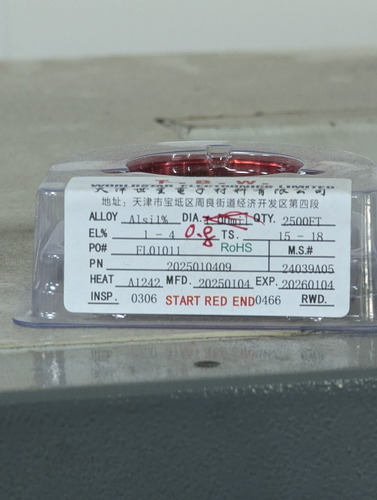
@Tim 'mithro' Ansell Wait no, on the pictures from the bonding factory, it's "AlSi" wire.
Tim 'mithro' Ansell 2026-05-01 1:53 a.m.
From the picture - AiSi1% at 0.8mil width. Apparently the 0.8mil wire is about 5x or 10x more expensive then the typical 1.0mil width bonding wire they use.
Avatar
Tim 'mithro' Ansell 2026-05-01 2:10 a.m.
BTW Everyone, I still remain very interested in trying to bring back gate arrays in the form of a base device created by wafer.space that then uses a single final coarse metal layer to do the final programming of the die - see some random ideas @ http://bit.ly/ws-gatearray-v1
GF180MCU Gate Array https://bit.ly/ws-gatearray-v1 Goal Create a good gate array which is programmable with post manufacturing additional of a metal layer in the 1-4um sizes. Specifications Final Metal Layer for Programming The goal is to have the gate array programmable by adding a single e...
👍 1
Avatar
that's a fun idea. was thinking about laser trimming earlier today but I like this idea more
Avatar
Avatar
Tim 'mithro' Ansell
@Noritsuna Imamura - Have you had a chance to give the ISHI bare die a probe? I would be interested to know how that goes! Please take lots of photos of your testing and share them too! I'm 100% sure others here would also be interested in your results. (edited)
Noritsuna Imamura 2026-05-01 2:26 a.m.
We plan to conduct tests using the probe. However, we expect that preparations will take a little more time. Once the measurements are taken, we plan to report the results.
Avatar
Avatar
BreakingTaps
that's a fun idea. was thinking about laser trimming earlier today but I like this idea more
Tim 'mithro' Ansell 2026-05-01 3:11 a.m.
@BreakingTaps - An alternative idea is to use something like lasers to cut paths rather than metal to add paths.
3:13 a.m.
@BreakingTaps - I feel like people like you, the Dr Semiconductor guy, and Hackerfab people could then do "ASICs" use these die in a few hour turn around.
Avatar
Avatar
Thorben
Got the naked dies a week ago already. Then just had to request access to our bonding machine and here we are.
yeah we have an Au ball bonder at work if we ever do a tapeout for a test project i can hand bond initial test ones
waferspace 1
Avatar
Avatar
Tim 'mithro' Ansell
@BreakingTaps - I feel like people like you, the Dr Semiconductor guy, and Hackerfab people could then do "ASICs" use these die in a few hour turn around.
Brian Swetland 2026-05-01 3:39 a.m.
a little RV32 core, a splash of SRAM, UART, SPI, and gate array fabric might make an interesting little chip
Avatar
Avatar
Tim 'mithro' Ansell
@BreakingTaps - I feel like people like you, the Dr Semiconductor guy, and Hackerfab people could then do "ASICs" use these die in a few hour turn around.
Yeah this is a really compelling idea, especially since you'd have 1000 to play around with. Will do more thinking on it!
Avatar
Avatar
Brian Swetland
a little RV32 core, a splash of SRAM, UART, SPI, and gate array fabric might make an interesting little chip
Tim 'mithro' Ansell 2026-05-01 3:57 a.m.
It seems like there is a lot of choice in the tiny silicon proven RISC-V cores like SERV and TinyQV and Fazy
Avatar
Avatar
Tim 'mithro' Ansell
BTW Everyone, I still remain very interested in trying to bring back gate arrays in the form of a base device created by wafer.space that then uses a single final coarse metal layer to do the final programming of the die - see some random ideas @ http://bit.ly/ws-gatearray-v1
Chips4Makers aka Staf Verhaegen 2026-05-01 9:35 a.m.
Most structured ASICs I have seen (eASIC, Triad Semiconductor) were using via layers for the customization layer(s). Via layers should also be able to be done faster for a maskless process like ebeam litho. One idea I had was to actually start from FPGA architecture but replace the storage cells in the LUTs and the routing cells with vias. (edited)
Avatar
Avatar
Tim 'mithro' Ansell
From the picture - AiSi1% at 0.8mil width. Apparently the 0.8mil wire is about 5x or 10x more expensive then the typical 1.0mil width bonding wire they use.
any idea on how the material cost compares to the capex/machine time there? Because without it's little to go on, sadly.
Avatar
Avatar
namibj
any idea on how the material cost compares to the capex/machine time there? Because without it's little to go on, sadly.
Tim 'mithro' Ansell 2026-05-01 10:47 a.m.
This was talking about the material cost of the actual wire (according to the bond house), not anything else.
Avatar
Yeah, I know. (It's just not at all actionable to any of us AFAIK without being able to see any perspective there.)
10:49 a.m.
doesn't have to be for sure tho
Avatar
Avatar
Chips4Makers aka Staf Verhaegen
Most structured ASICs I have seen (eASIC, Triad Semiconductor) were using via layers for the customization layer(s). Via layers should also be able to be done faster for a maskless process like ebeam litho. One idea I had was to actually start from FPGA architecture but replace the storage cells in the LUTs and the routing cells with vias. (edited)
Tim 'mithro' Ansell 2026-05-01 10:49 a.m.
Yes, but the current "standard" way of doing most structured ASICs / gate array devices has lead to them no longer being manufactured / killed them -- so following down that path seems like not the best idea 🙂
Avatar
Hey folks! Quick GF180/wafer.space question: are there any usable on-chip NVM options for open submissions, like MTP/YMTP, or should I design assuming no embedded NVM and boot from external QSPI flash? Mostly looking for practical experience / gotchas, not an official commitment. Thanks!
Avatar
Avatar
Zhekar1998
Hey folks! Quick GF180/wafer.space question: are there any usable on-chip NVM options for open submissions, like MTP/YMTP, or should I design assuming no embedded NVM and boot from external QSPI flash? Mostly looking for practical experience / gotchas, not an official commitment. Thanks!
Somebody made an OTP efuse compiler, iirc the first tapeout failed due to a missing power connection
3:43 p.m.
i dont know if the next revision is back yet
3:43 p.m.
but AFAIK gf supports fuses on this node
3:43 p.m.
its the kind of thing you would use for trim settings not firmware
Avatar
Avatar
azonenberg
Somebody made an OTP efuse compiler, iirc the first tapeout failed due to a missing power connection
Oh yeah, sounds painful 😅 are there any other options for rewritable NVM though? (not OTP)
Avatar
Not to my knowledge. Flash etc needs a lot of extra masks that add significant cost
4:01 p.m.
There may be a ROM compiler, i know folks were working on them but not sure what's been silicon proven so far
4:02 p.m.
but if you need it field programmable just hang a spi flash off they're cheap
Avatar
for me its some complicated to have 3 different flash, but for first demonstrator maybe its best option) (edited)
Avatar
Avatar
azonenberg
Somebody made an OTP efuse compiler, iirc the first tapeout failed due to a missing power connection
Egor Lukyanchenko 2026-05-01 5:12 p.m.
It was me :). New revision is currently being wirebonded, so in a couple of weeks we'll see if it works.
👍 1
Avatar
Avatar
Tim 'mithro' Ansell
Yes, but the current "standard" way of doing most structured ASICs / gate array devices has lead to them no longer being manufactured / killed them -- so following down that path seems like not the best idea 🙂
what's the tl;dr here? Just not commercially viable vs taping out your own chip? I'm not super familiar with the history of these devices
Avatar
Avatar
BreakingTaps
what's the tl;dr here? Just not commercially viable vs taping out your own chip? I'm not super familiar with the history of these devices
AFAIK people use FPGAs and probably modern scaling's issues with leakage power discouraging from doing things the old way.
👍 1
Avatar
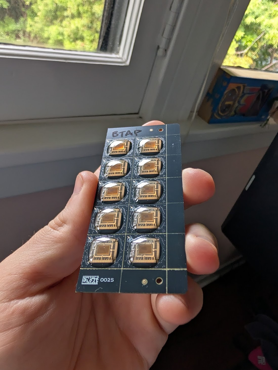
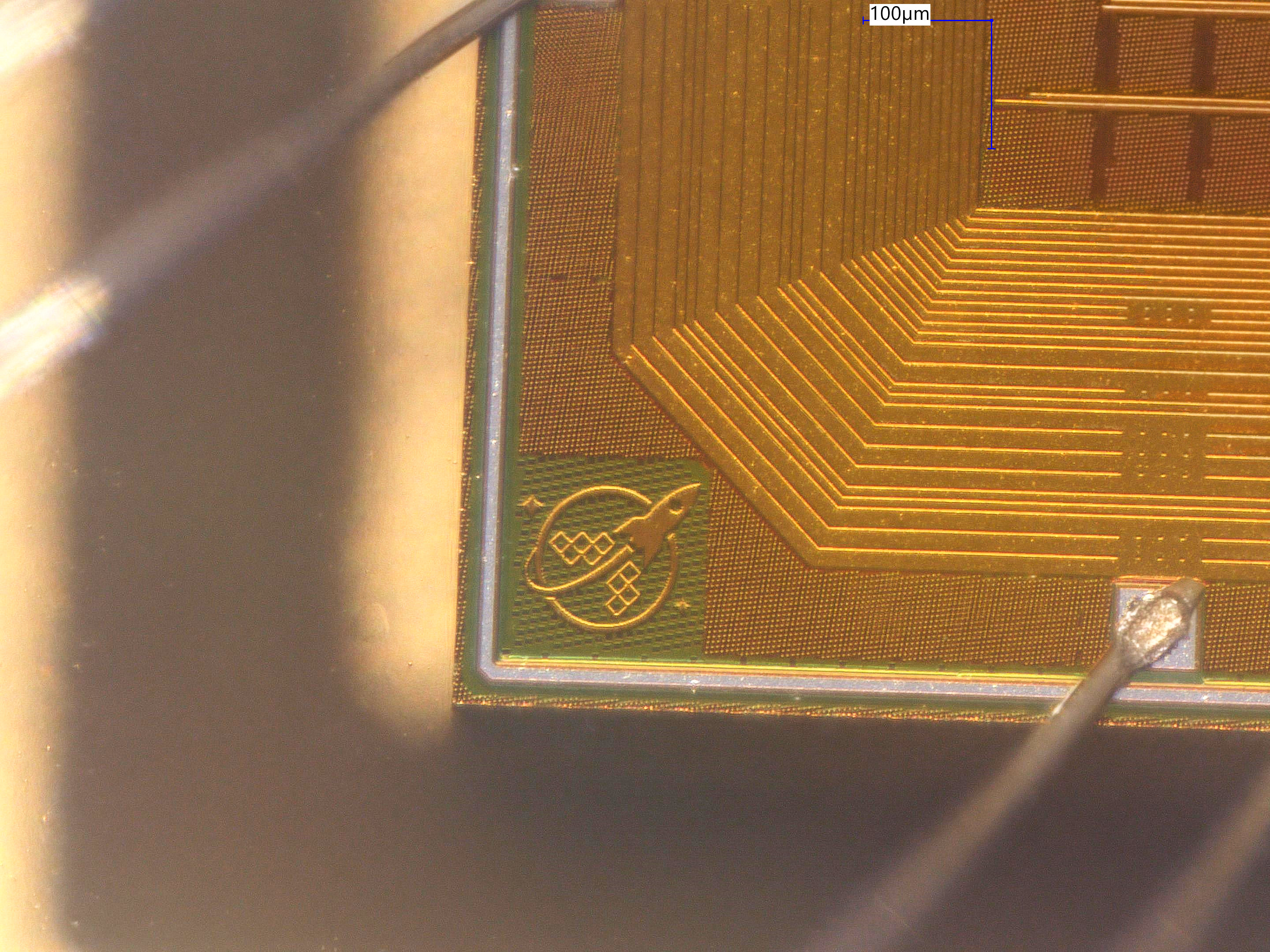
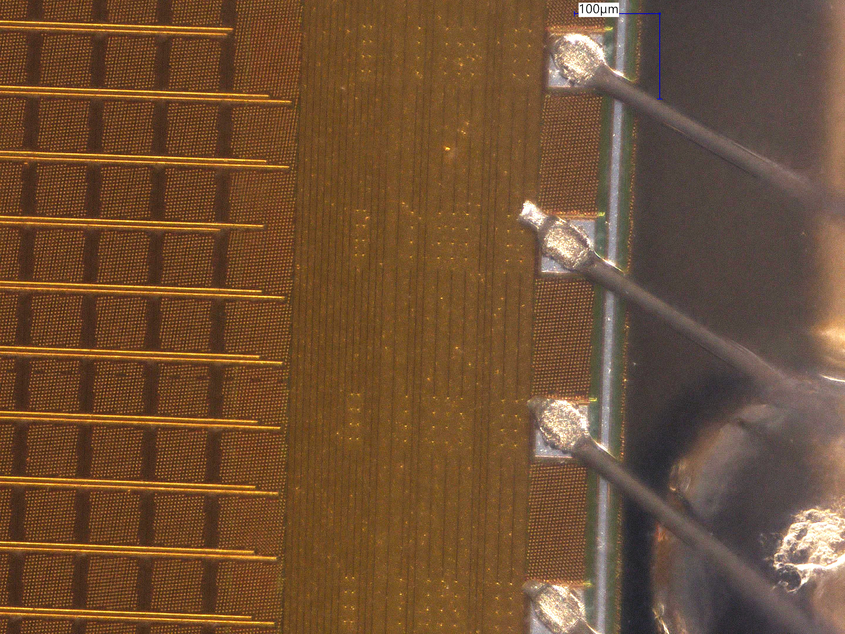
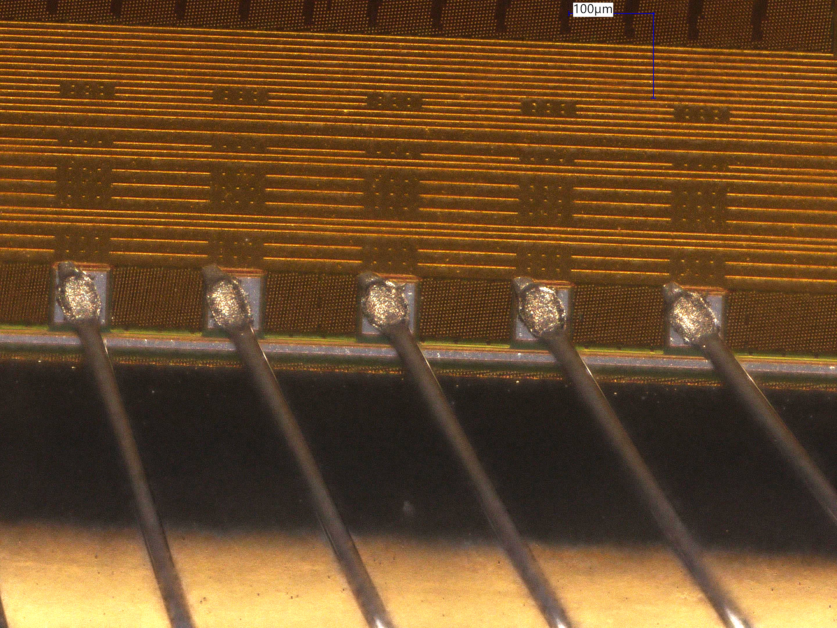
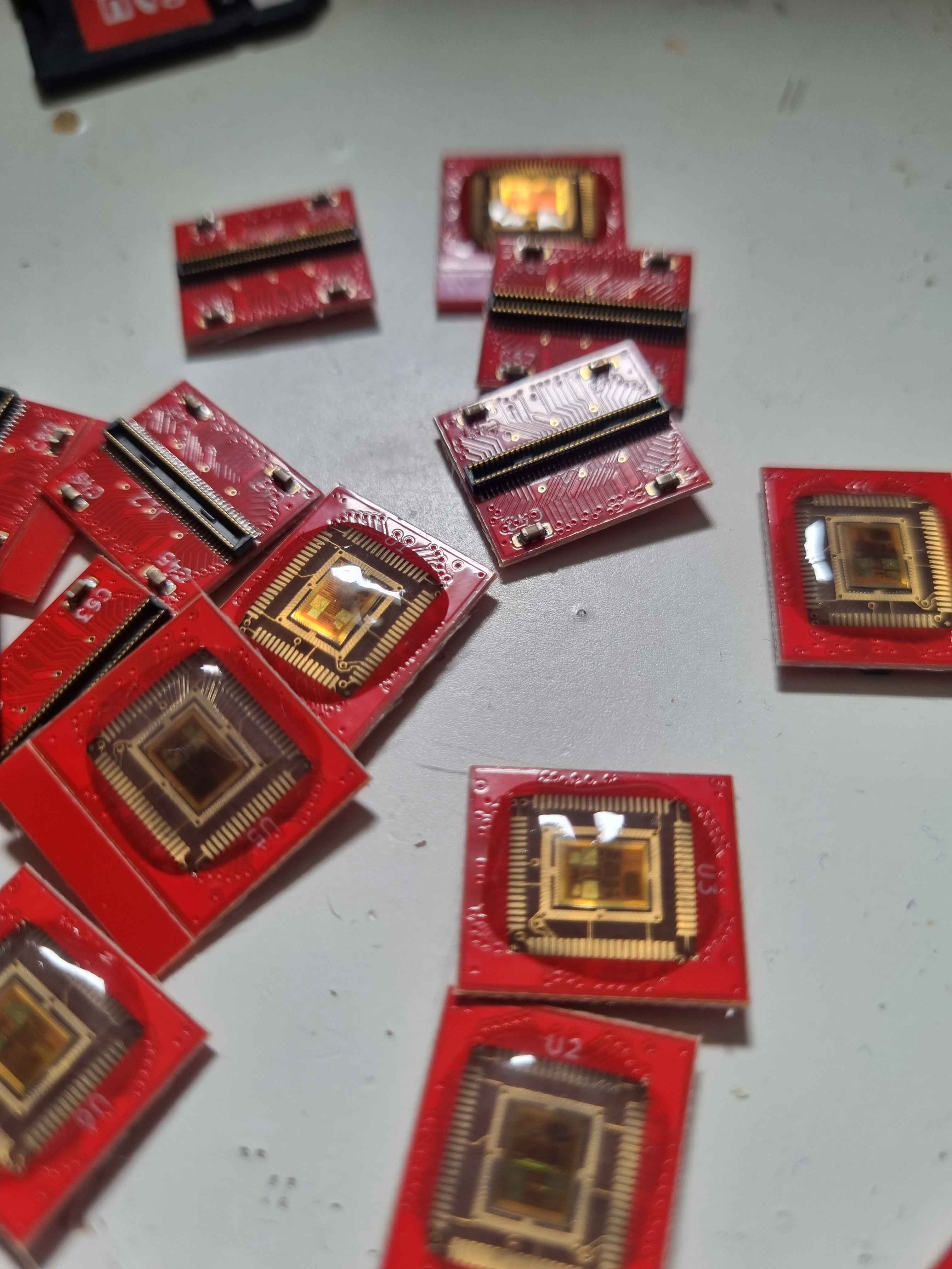
Some photos of my COB chips
🔥 3
🎉 6
waferspace 1
Avatar
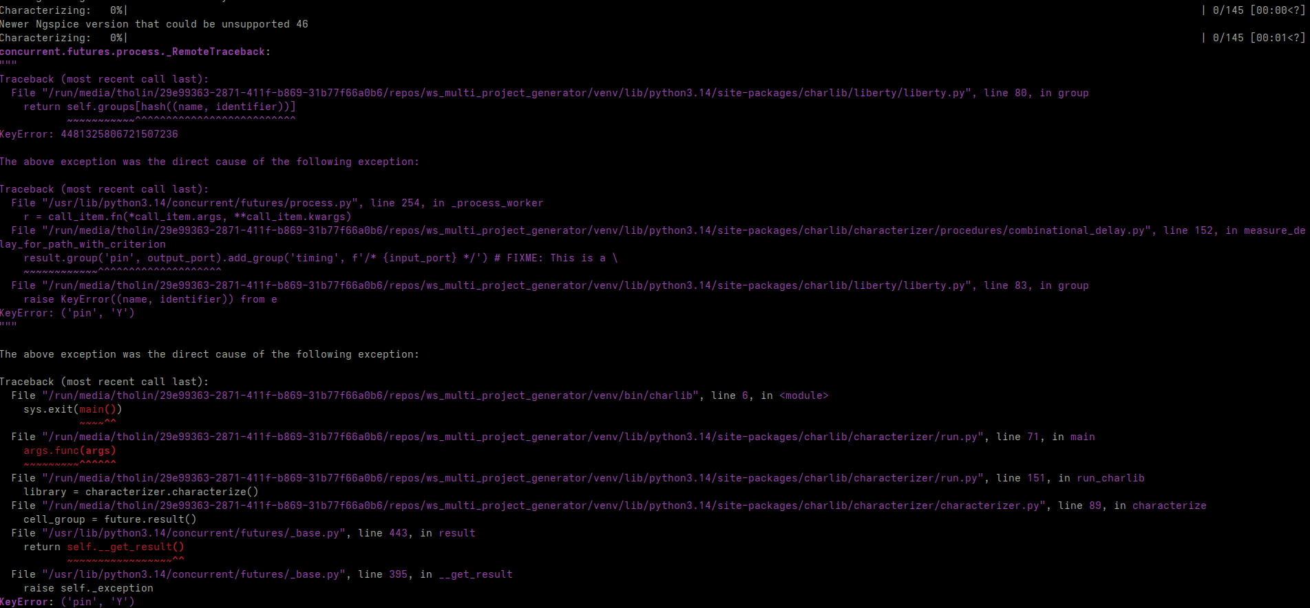
I’ve been trying to get charlib to work for me since last year, but its still crashing with impossible to interpret errors even though I’m sure I’m doing everything right
Avatar
Avatar
BreakingTaps
Some photos of my COB chips
Tim 'mithro' Ansell 2026-05-02 2:42 a.m.
Very cool pictures!
Avatar
Avatar
BreakingTaps
what's the tl;dr here? Just not commercially viable vs taping out your own chip? I'm not super familiar with the history of these devices
Tim 'mithro' Ansell 2026-05-02 2:54 a.m.
My theories on why gate arrays went extinct are the following:
  • Gate arrays meant dealing with a silicon foundry. Once you have gone through the huge effort of dealing with a silicon foundry, then the performance improvements of going full custom seem higher ROI.
  • Most groups focused on trying to make gate arrays competitive with custom silicon design from a PPA rather than focus on time to market and customizability.
  • Foundries still wanted to own the customization step, not just the production of the starting gate array material.
  • Gate array refused to learn from what FPGA people where doing.
  • CPUs & FPGAs got a lot better.
  • The industry is so focused on volume and scaling that gate arrays don't make sense when you assume every project needs to sell 1 million units before it breaks even.
  • Maskless solutions in foundries never took off because again the industry is so focused on huge scale.
  • Everyone one was focused on the silicon side and did not invest in the software side.
I haven't done an exhaustive search, but a lot of the gate array examples I have seen had the silicon wafers prepared to the end of FEOL and then used highest density metal for configuration. This (maybe) makes sense if you are trying to do gate arrays of transistors and form them into standard cells and SRAM blocks but also means they still take quite a long time to be made (IE O(months) rather than O(hours)). Basically, nobody was focused on:
  • How to I make gate arrays cheap and fast for the small run or even individual unit use case.
  • Providing prebuilt items like SRAM blocks, wide busses, etc.
  • Focused on enabling as many different solutions for programmability.
Avatar
Avatar
Tim 'mithro' Ansell
My theories on why gate arrays went extinct are the following:
  • Gate arrays meant dealing with a silicon foundry. Once you have gone through the huge effort of dealing with a silicon foundry, then the performance improvements of going full custom seem higher ROI.
  • Most groups focused on trying to make gate arrays competitive with custom silicon design from a PPA rather than focus on time to market and customizability.
  • Foundries still wanted to own the customization step, not just the production of the starting gate array material.
  • Gate array refused to learn from what FPGA people where doing.
  • CPUs & FPGAs got a lot better.
  • The industry is so focused on volume and scaling that gate arrays don't make sense when you assume every project needs to sell 1 million units before it breaks even.
  • Maskless solutions in foundries never took off because again the industry is so focused on huge scale.
  • Everyone one was focused on the silicon side and did not invest in the software side.
I haven't done an exhaustive search, but a lot of the gate array examples I have seen had the silicon wafers prepared to the end of FEOL and then used highest density metal for configuration. This (maybe) makes sense if you are trying to do gate arrays of transistors and form them into standard cells and SRAM blocks but also means they still take quite a long time to be made (IE O(months) rather than O(hours)). Basically, nobody was focused on:
  • How to I make gate arrays cheap and fast for the small run or even individual unit use case.
  • Providing prebuilt items like SRAM blocks, wide busses, etc.
  • Focused on enabling as many different solutions for programmability.
Egor Lukyanchenko 2026-05-02 4:25 a.m.
I would say that gate arrays might be interesting if they'll be available with a rapid PCB prototyping kind of "programming" service. Something like a TinyTapeout, but with a turnaround time of about a week and a cost of around 200$/10 units might find its users. The gate array should have something like 20% of logic density if compared with a full custom layout on the same technology, so WS full slot based GA will be large enough to fit a decent design even with around half of the area reserved for the fixed logic like a CPU and SRAM. (edited)
Avatar
Tim 'mithro' Ansell 2026-05-02 6:27 a.m.
@Egor Lukyanchenko - If we could prove a wafer.space die could be programmed using something like the HackerFab Stepper (which is like ~$10k USD) and each wafer.space die is $7 USD a part, then $200 USD for 10 units in 1-2 weeks kind of seems like something someone could have a small side business doing. (10*$7 == $70 USD for the die leaves $130 USD to cover the time and HackerFab stepper investment).
Avatar
Egor Lukyanchenko 2026-05-02 7:08 a.m.
@Tim 'mithro' Ansell
If we could prove a wafer.space die could be programmed using something like the HackerFab Stepper
If the spatial resolution of the HackerFab machine for adding the top metal is known, the achievable logic density of such GA could be easily estimated. The software flow based on Yosys+OpenROAD appears to be doable, as the only truly custom step is constrained placement, which is closer to the FPGA than to ASIC. But designing a “good” GA architecture, which could achieve a reasonable density and speed, will take quite some time, I think.
(10*$7 == $70 USD for the die leaves $130 USD to cover the time and HackerFab stepper investment)
That is where my 20$/piece price came from :).
Avatar
Avatar
Egor Lukyanchenko
@Tim 'mithro' Ansell
If we could prove a wafer.space die could be programmed using something like the HackerFab Stepper
If the spatial resolution of the HackerFab machine for adding the top metal is known, the achievable logic density of such GA could be easily estimated. The software flow based on Yosys+OpenROAD appears to be doable, as the only truly custom step is constrained placement, which is closer to the FPGA than to ASIC. But designing a “good” GA architecture, which could achieve a reasonable density and speed, will take quite some time, I think.
(10*$7 == $70 USD for the die leaves $130 USD to cover the time and HackerFab stepper investment)
That is where my 20$/piece price came from :).
Tim 'mithro' Ansell 2026-05-02 11:47 a.m.
Yeap, so it just needs someone to "do the work" 🙂
🙂 1
Avatar
I agree - if there was a way to one-time program gate arrays (post-production), that would be popular and useful, and a good use for any excess capacity.
Avatar
The industry is so focused on volume and scaling that gate arrays don't make sense when you assume every project needs to sell 1 million units before it breaks even.,
Yeah this is overall sooooo endemic. Really hurts innovation, obviously.
Avatar
Avatar
Tim 'mithro' Ansell
@Egor Lukyanchenko - If we could prove a wafer.space die could be programmed using something like the HackerFab Stepper (which is like ~$10k USD) and each wafer.space die is $7 USD a part, then $200 USD for 10 units in 1-2 weeks kind of seems like something someone could have a small side business doing. (10*$7 == $70 USD for the die leaves $130 USD to cover the time and HackerFab stepper investment).
afaik the biggest spenditure would actually be time, and space
3:01 p.m.
You cannot guarantee a scalable chip if you don't have a reliable cleanroom, and you need to have not only the litography machine (which, granted, tens to be the most expensive machine), but also a way to bake the wafers, a way to supply said wafers, a way to deal with potentially dangerous chemicals, a way to inspect the chips, and you need to do all this with reproducibility always in mind
3:03 p.m.
To be fair as they do advertise on the Hacker Fab website, they're quickly refining the process and the price to manage making low-volume chips is quickly going down (edited)
3:04 p.m.
I myself know I want to make a Hacker Fab myself, for my low-volume ASICs, but I would never feel comfortable selling at any scale larger than 5 or 10 of them to individuals
Avatar
Avatar
Dory
You cannot guarantee a scalable chip if you don't have a reliable cleanroom, and you need to have not only the litography machine (which, granted, tens to be the most expensive machine), but also a way to bake the wafers, a way to supply said wafers, a way to deal with potentially dangerous chemicals, a way to inspect the chips, and you need to do all this with reproducibility always in mind
Tim 'mithro' Ansell 2026-05-02 3:31 p.m.
I'm actually skeptical that a reliable cleanroom is needed when you are doing stuff on individual chips and something like a single 5um or 10um metal layer. Plus if you have a 1 in 10 failure rate, you have only lost like $7 USD for that failure.
3:36 p.m.
A semiconductor fab wouldn't accept a 10% failure rate per metal layer because they need to do like 5 or more metal layers and on failure you just burnt a an almost complete wafer. But here you only have 1 layer to do and a failure is only negatively impacting a pretty cheap cost.
Avatar
Hmmm that is fair
3:38 p.m.
Afaik the Hacker Fab project actually got away with just using a plasma cleaner and execising caution
3:39 p.m.
In practice a good solvent choice might even be abe to get rid of most meaningful aberrations
Avatar
Tim 'mithro' Ansell 2026-05-02 3:39 p.m.
It's risk verse reward -- If I'm spending $X billions to build a fab, then I'm going to be a bit more demanding than if I'm just spending $10k USD 🙂
Avatar
of course, that is fair! But you also have to take into account that the difference too is in the fact that the one assembling a billion-worth fab is a multibillion company, whilst the 10k fab is an individual
3:41 p.m.
And the multibillion company already has a market and investors, so it can ensure that the projects will see the light of day
3:41 p.m.
I can guarantee that if I also had investors and knew I'd make at least as much as I spend on making a fab setup, I would just, make the fab
3:41 p.m.
But it's a bit of a risky gamble
Avatar
Avatar
Dory
You cannot guarantee a scalable chip if you don't have a reliable cleanroom, and you need to have not only the litography machine (which, granted, tens to be the most expensive machine), but also a way to bake the wafers, a way to supply said wafers, a way to deal with potentially dangerous chemicals, a way to inspect the chips, and you need to do all this with reproducibility always in mind
Those minimal fabs try to solve this by fitting the equipment in a small, highly automated volume instead of maintaining a full cleanroom. I think you can make this idea work.
Avatar
Hmmm yeah that definitely sounds like a pretty plausible idea
3:51 p.m.
Yeah and the market can't be too hard to find
Avatar
Avatar
Tim 'mithro' Ansell
I'm actually skeptical that a reliable cleanroom is needed when you are doing stuff on individual chips and something like a single 5um or 10um metal layer. Plus if you have a 1 in 10 failure rate, you have only lost like $7 USD for that failure.
yeah single layer is not that intense cleanroom; also you just use essentially a line of laminar flow hoods; you don't need the humans in the clean part of the room
Avatar
Tim 'mithro' Ansell 2026-05-02 3:52 p.m.
While it is a definitely a privileged position, I'm sure that there are a lot of people who have $10k spare compared to multibillion dollar companies willing to risk building semiconductor fab.
Avatar
5 to 7$ for a chip, custom made with at most 6 weeks lead time, seems like a great offer I know I wouldn't pass on
Avatar
Avatar
Dory
Yeah and the market can't be too hard to find
Medical sensors need the analog capacity, and subthreshold design for ULP as well
Avatar
Avatar
Tim 'mithro' Ansell
While it is a definitely a privileged position, I'm sure that there are a lot of people who have $10k spare compared to multibillion dollar companies willing to risk building semiconductor fab.
Also small businesses might benefit from this
3:53 p.m.
well there is a whole small business in and of itself
Avatar
If we can find a way of doing heterogeneous packaging the opportunities will explode, which I know @namibj was interested in
Avatar
Avatar
Christopher
If we can find a way of doing heterogeneous packaging the opportunities will explode, which I know @namibj was interested in
It can probably be done by using "internal pads", kind of how PCB stacking was done during the transition to transistor logic
3:56 p.m.
I've seen a few good PCBs, if on the older side, that used this to their advantage, so I don't see why it couldn't be done with silicon
3:58 p.m.
My entrepenurial and experimental sides are coalescing too much over this idea and I feel the pull to make a crowdsupply campaign to try and get an "indie semiconductor fab" to be a real thing /hj
Avatar
Avatar
Dory
I've seen a few good PCBs, if on the older side, that used this to their advantage, so I don't see why it couldn't be done with silicon
Share?
Avatar
Avatar
Dory
My entrepenurial and experimental sides are coalescing too much over this idea and I feel the pull to make a crowdsupply campaign to try and get an "indie semiconductor fab" to be a real thing /hj
Check the link Tim sent, its something people are working on for sure
Avatar
Avatar
namibj
Share?
Uhhh I have one very good example on the workshop. It used to be on the innards of a locomotive when the whole thing about "electronic security" was starting to be a thing
4:05 p.m.
Iirc they have various copper pillars that are bolted in between two PCBs and they're used to transmit data directly between the 2-layer PCBs
4:05 p.m.
Well I say two later but it's just a one-sided copper substrate
Avatar
Avatar
Christopher
Check the link Tim sent, its something people are working on for sure
Yeah I know and that's the thing, it's something I'm definitely interested on trying for myself anyways so might as well make my thesis and a business out of it xd
Avatar
Tim 'mithro' Ansell 2026-05-02 4:17 p.m.
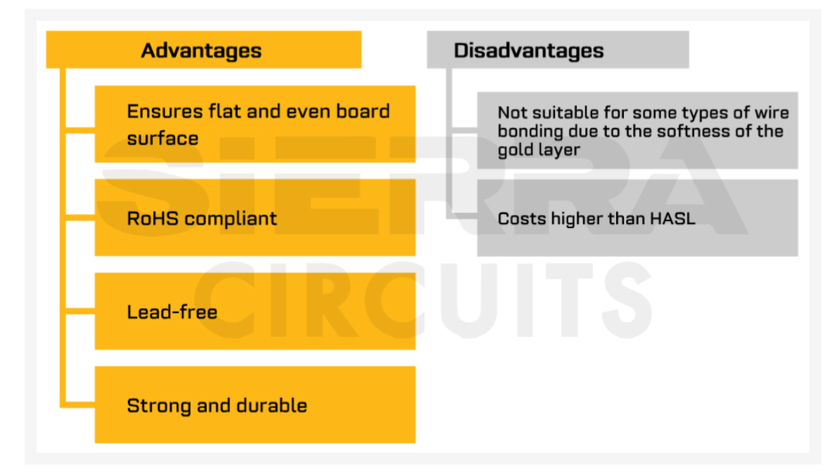
I'm trying to convince PCBA houses to offer wire bonding as part of their PCBA services which opens up a way to integrate a bunch of devices together.
Avatar
Yeah the bad thing is that that would be a costly service not many at-scale clients would use
4:18 p.m.
JLC for example earns most of their money off of medium-batch PCBA and large-scale PCB manufacture
Avatar
Tim 'mithro' Ansell 2026-05-02 4:18 p.m.
PCBs where once a costly service 🙂
Avatar
Everything else they offer is just either cheap to have running or can be easily made with the otherwise defunct machines involved
Avatar
Avatar
Tim 'mithro' Ansell
PCBs where once a costly service 🙂
Yeah of course! But that didn't stop them from being popular!
4:19 p.m.
Wire-bonding is still a very niche process except for very specific applications, and the companies that can afford to supply dies can already afford to bond and coat it themselves
4:20 p.m.
So you try telling the JLC executives that if they drop a bunch of money at adding another service, it might be profitable after... Well, between a long time and never
Avatar
Tim 'mithro' Ansell 2026-05-02 4:24 p.m.
@Dory - Don't know about JLC, but a number of other groups (like PCB Way) already have wire bonding machine -- they just don't offer access to those machines to non-chinese customers today because they don't have a way to do automated quoting like they can with PCB/PCBA.
Avatar
Ahhh that is very fair
4:25 p.m.
I wouldn't have thought that is the case, see
4:25 p.m.
But then again it makes sense too
4:26 p.m.
Though I'm guessing my argument for why you wouldn't do it small scale still applies
4:27 p.m.
It's so costly to have a few bare dies shipped to china, pay full time engineer hours for operation of a machine that can easily take an hour to be done, and needs their full attention, and then to pot it an ensure it will last
4:27 p.m.
But it'd be awesome to see it become a thing, so I'll pray for your success from the sidelines hehe
Avatar
Avatar
Dory
Uhhh I have one very good example on the workshop. It used to be on the innards of a locomotive when the whole thing about "electronic security" was starting to be a thing
Workshop?
Avatar
Avatar
Dory
Wire-bonding is still a very niche process except for very specific applications, and the companies that can afford to supply dies can already afford to bond and coat it themselves
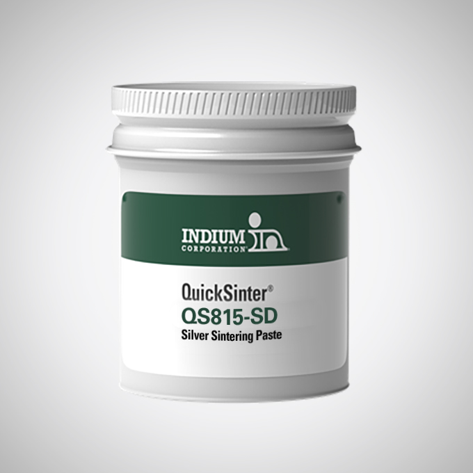
I'm happy the GaN are lateral devices, so unlike the SiC JFETs from (formerly) UnitedSiC, no need for silver sintering.
4:35 p.m.
Though I should look at whether that (low temperature silver sintering) can do enough resolution to work for flip chip bonding of wafer.space dies without (much/expensive) post-processing.
Avatar
Avatar
namibj
Workshop?
Yeah I have a little workshop on the other side of town. Well it's my father's but we kinda share
4:36 p.m.
It's more of a... Dump than anything else
4:36 p.m.
I have a few old electronics and mechateonics stuff hanged up
Avatar
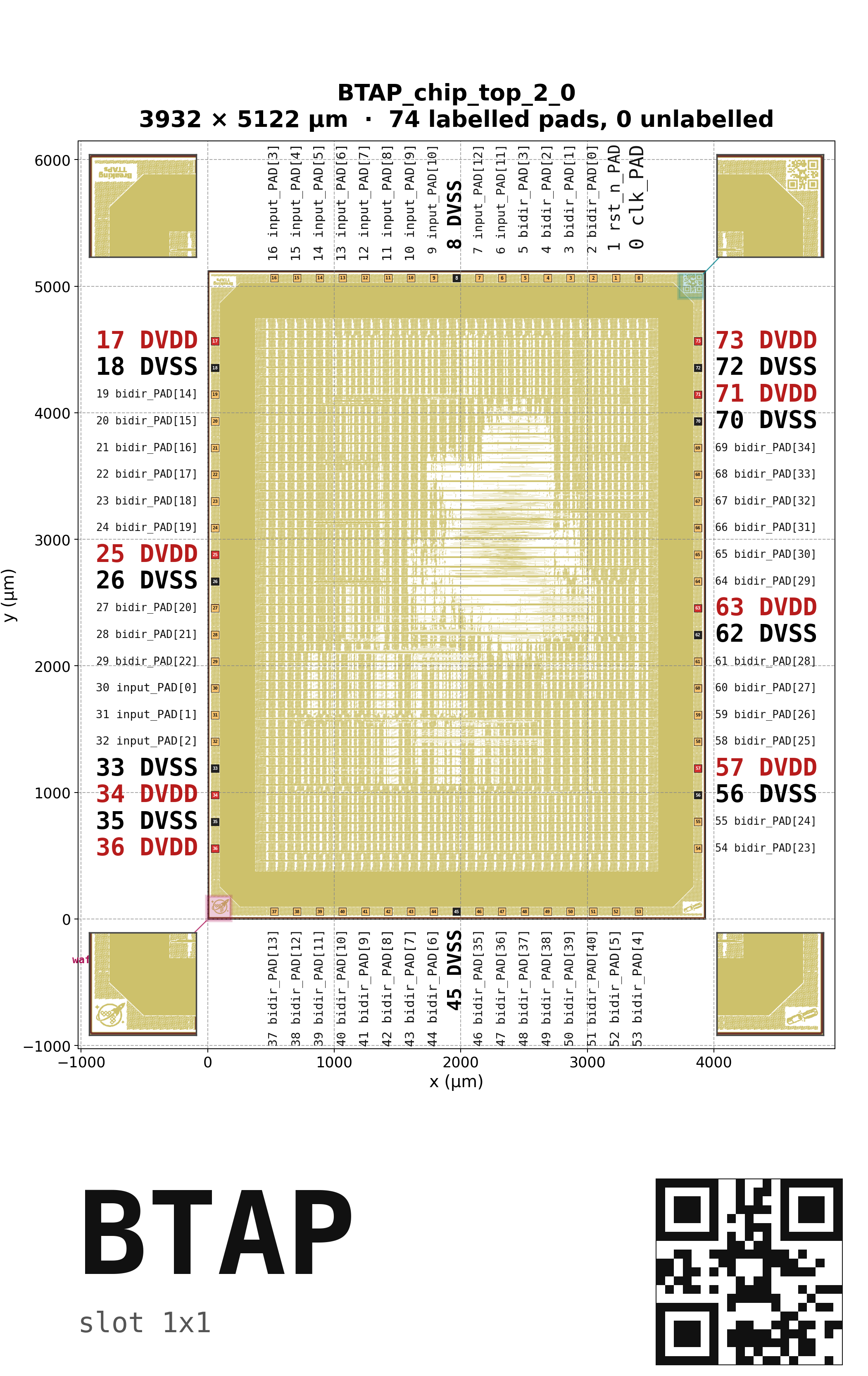
A tool to generate multi-project dies for wafer.space shuttles - AvalonSemiconductors/ws_multi_project_generator
👍 1
4:52 p.m.
Still needs docs, but it is functional
4:53 p.m.
Allows for automatic generation of multi-project setups with all 50 GPIOs shared between the projects, up to 15 projects
4:53 p.m.
Digital only
4:54 p.m.
One possible application for this is it to further reduce tape-out cost by carrying multiple different people’s projects on one die
5:05 p.m.
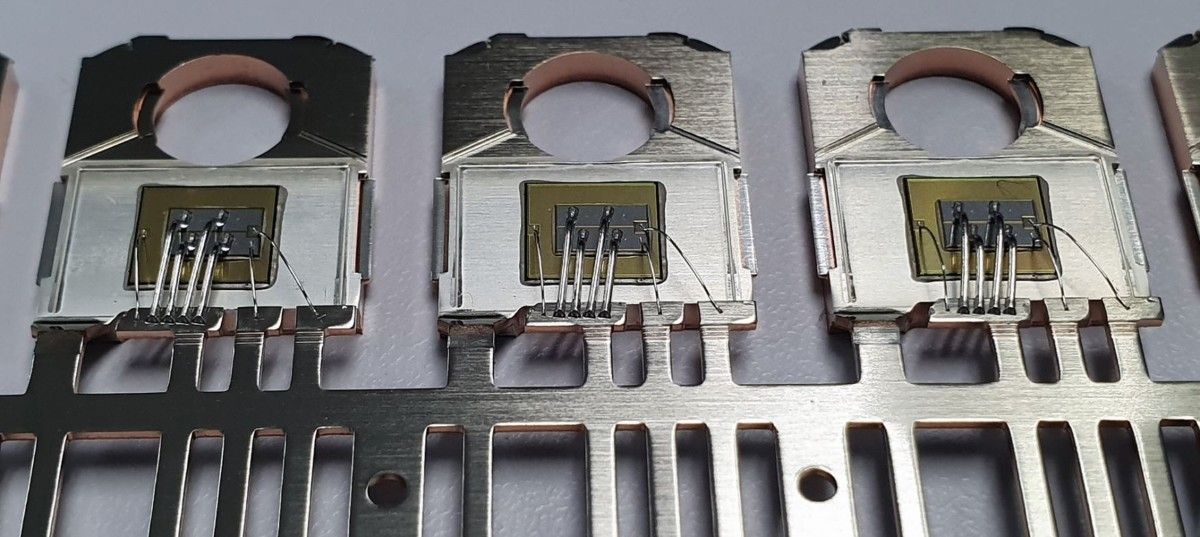
I'd probably be able to bankroll a single one of these dies worth of wafer.space next year if we have figured out a way to bond the gate drive current to the wafer.space die for it. I'd actually assume it should be possible to do without flip-chip but instead "just" using the kind of thick rectangular al bond "wire" they use for e.g. the TO-247 packages of the UnitedSiC Gen4 cascodes:
5:06 p.m.
5:08 p.m.
That's a large SiC vertical jfet drain down with a 30V vertical silicon mosfet drain sintered to the SiC source; the SiC gate is the tiny pad off to the left; then the mosfet has a kelvin gate bonded out (two legs of the TO-247 for gate purposes, one is source the other gate) and ofc the fat source bonding for the load current.
❤️ 1
Avatar
Tim 'mithro' Ansell 2026-05-03 3:28 a.m.
Very cool! I'm very on board with promoting this work and having people hiring your services to help people afford slots by sharing.
Avatar
Avatar
namibj
Click to see original message
Tim 'mithro' Ansell 2026-05-03 3:34 a.m.
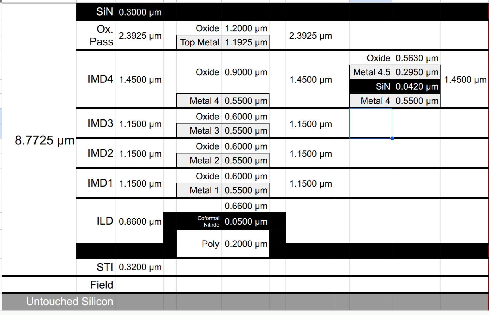
I would potentially be interested in exploring how a pattern like this on the top metal could be used for bonding directly rather than needing bond wires (IE provide free silicon if there is spare/leftover space on the shuttle).
Avatar
Avatar
Tim 'mithro' Ansell
I would potentially be interested in exploring how a pattern like this on the top metal could be used for bonding directly rather than needing bond wires (IE provide free silicon if there is spare/leftover space on the shuttle).
non-wedge-bonding should likely be fine with active area underneath; for merely testing the flip-chip tactic(s) as-such it shouldn't really need more than.... wiring a normal IO pad to a suitably large pad in a more central location on the die? I don't know what non-customer-GDS slices you're planning to have for Run2, but later this month or possibly early next month I'd be up for making a more concrete proposal/"pitch deck" with the ESD aspects researched out for such an option/opportunity. If that's what you're approximately thinking of here?
Avatar
Avatar
namibj
non-wedge-bonding should likely be fine with active area underneath; for merely testing the flip-chip tactic(s) as-such it shouldn't really need more than.... wiring a normal IO pad to a suitably large pad in a more central location on the die? I don't know what non-customer-GDS slices you're planning to have for Run2, but later this month or possibly early next month I'd be up for making a more concrete proposal/"pitch deck" with the ESD aspects researched out for such an option/opportunity. If that's what you're approximately thinking of here?
Tim 'mithro' Ansell 2026-05-03 3:44 a.m.
I don't really care about being pitched too, I'm just interested in helping promote the exploration of ideas which might help reduce cost further by eliminating wire bonding and such.
Avatar
Avatar
Tim 'mithro' Ansell
I don't really care about being pitched too, I'm just interested in helping promote the exploration of ideas which might help reduce cost further by eliminating wire bonding and such.
no I mean regarding a concrete concept of how to potentially explore how such a pattern on top metal could be used for flip chip bonding, without having to dedicate the flip chip pad's top metal occupied area across all layers (e.g. it should only need a fraction of the active area underneath, unless we assume particularly advanced fine-pitch flip-chip techniques)
3:48 a.m.
oh sorry, I again misread; I thought you said "I don't really recall being pitched to"
3:51 a.m.
I won't have any of the analog PA things (needed to make integration with one of those GaN chips useful) ready in time for Run2, but there's other things that could be bonded to a Run2 die to trial the bonding process itself.
Avatar
Tim 'mithro' Ansell 2026-05-03 3:51 a.m.
I also don't need to necessarily understand everything either :-). Throwing stuff against the wall and seeing what sticks is part of the idea behind trying to make things continually cheaper.
Avatar
Avatar
namibj
I won't have any of the analog PA things (needed to make integration with one of those GaN chips useful) ready in time for Run2, but there's other things that could be bonded to a Run2 die to trial the bonding process itself.
Tim 'mithro' Ansell 2026-05-03 3:54 a.m.
Filling the die with different types of silicon capacitors (MIM, MOS & MOM) and maybe even some efuses with a very simple 1-wire core so info about lot number, wafer number, wafer position could be burned into the device would be perfectly resonable to me.
Avatar
Yeah, I thought to mean that for whoever would try to make more productive use of the lower layers in that area (those not used by the ESD structures), to "convince" them that this upper layer structure with a little bit of active pad structure underneath would be harmless enough to include. Could be with some new sram macro trial or something more experimental than normal slice usage, I'd assume.
Avatar
Avatar
Tim 'mithro' Ansell
Filling the die with different types of silicon capacitors (MIM, MOS & MOM) and maybe even some efuses with a very simple 1-wire core so info about lot number, wafer number, wafer position could be burned into the device would be perfectly resonable to me.
Oh yeah it should be perfectly fine to trial efuse designs (well, EPROM as a general concept, I don't mean the specific UV-erasable variety) in the spare active area under such a pad.
Avatar
Avatar
namibj
Oh yeah it should be perfectly fine to trial efuse designs (well, EPROM as a general concept, I don't mean the specific UV-erasable variety) in the spare active area under such a pad.
Tim 'mithro' Ansell 2026-05-03 4:02 a.m.
GF180MCU Silicon Capacitor Goal Create software which is able to generate a "maximal silicon capacitor" for a given configuration. Specifications GDSFactory https://gdsfactory.github.io/gdsfactory/ Uses AI to tune the capacitor capacity (IE the shapes of structures). https://gdsfactory.github...
Avatar
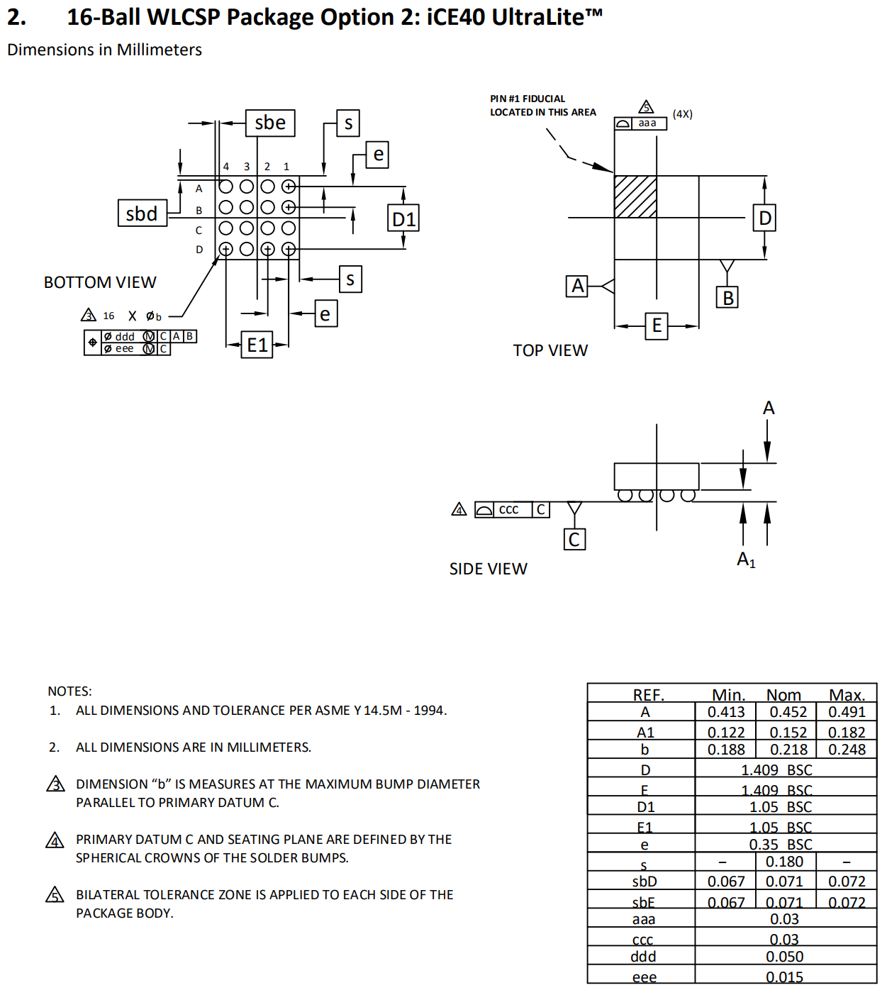
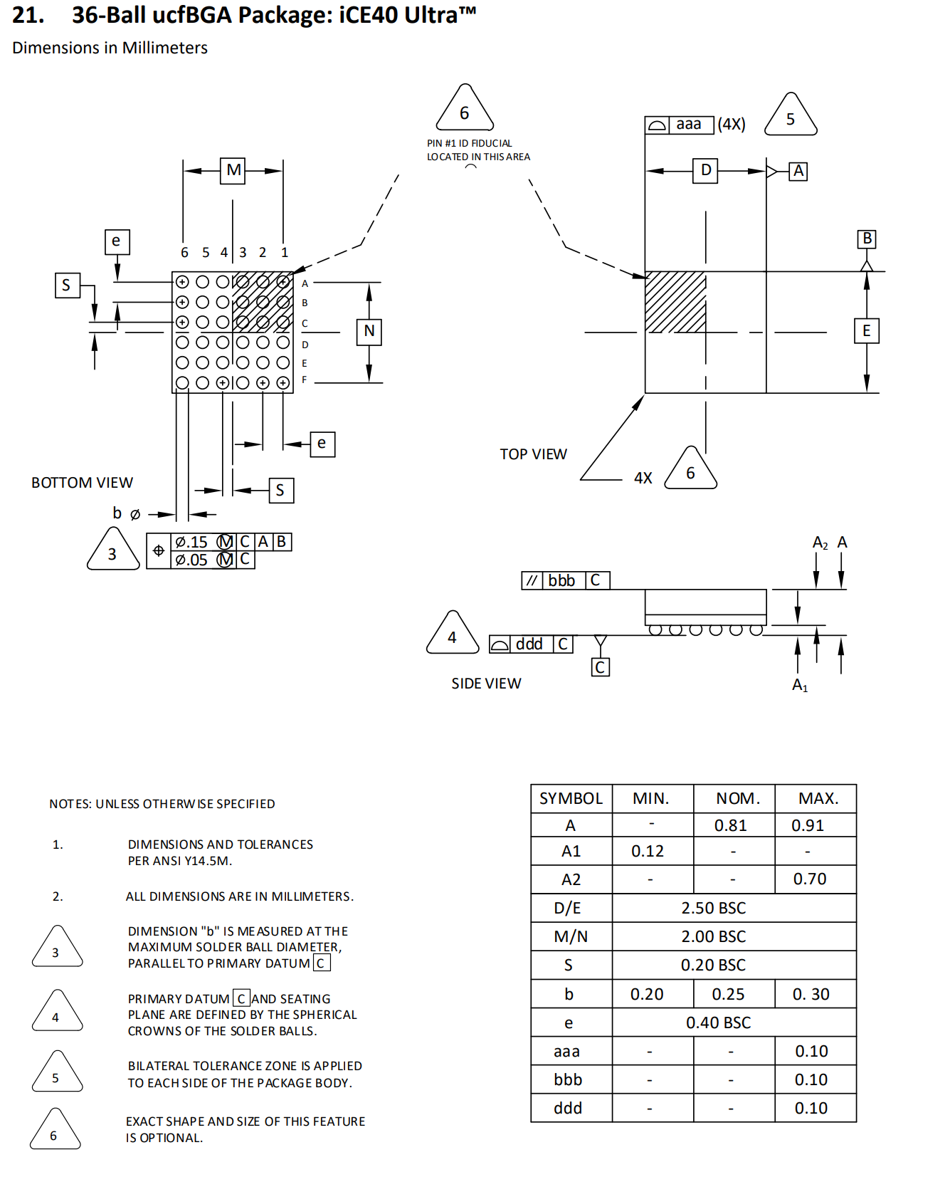
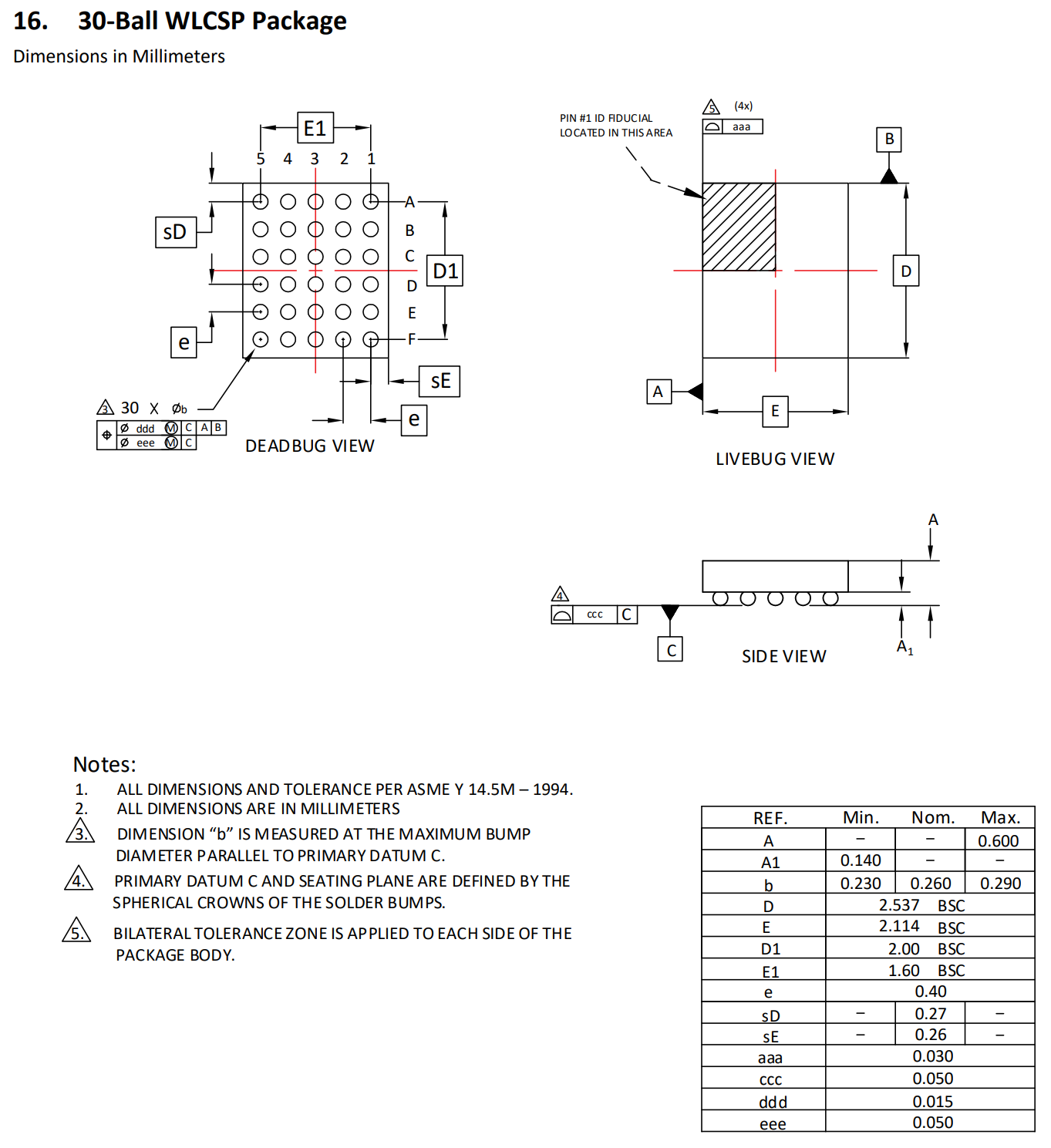
in lieu of anything better I'd suggest an ice40ul1k-swg16 or a ice40up3k/ice40up5k (I heard they're the same; the former just isn't sold in the QFN48 package)
4:08 a.m.
but yeah silicon capacitor pinned raw out to the pads could be something; antenna diodes are used in avalanche connection to be reverse-biased in normal operation, right?
4:13 a.m.
sorry this was the one for the up5k; the above ones were just the ultra lite vs. ultra [non-lite]
Avatar
Tim 'mithro' Ansell 2026-05-03 5:16 a.m.
I'm currently working to source known-good-die of ice40up5k through my Lattice contacts.
Avatar
Brian Swetland 2026-05-03 5:18 a.m.
I miss the days when those parts were $4-5 in handful quantities
Avatar
Tim 'mithro' Ansell 2026-05-03 5:19 a.m.
@Brian Swetland - How much are they these days? I've generally gotten them at $1-$2 USD per part in the past (but I've been buying multiple full reels at a time).
Avatar
Brian Swetland 2026-05-03 5:20 a.m.
looks like cut tape, single digits is $10-11 on digikey/mouser... down to $8-9 in the hundreds
5:21 a.m.
I assume some combo of popularity and the parts crunch that kicked off a bit into the pandemic were contributing factors here
5:22 a.m.
being able to buy 5-10 for ~$4 each was hobbyist fpga nirvana back when the yosys/nextpnr tooling was getting solid
Avatar
Avatar
Tim 'mithro' Ansell
Yes, but the current "standard" way of doing most structured ASICs / gate array devices has lead to them no longer being manufactured / killed them -- so following down that path seems like not the best idea 🙂
Chips4Makers aka Staf Verhaegen 2026-05-03 4:08 p.m.
I don't believe the reason for example eASIC in the end failed was technical but financial, e.g. investors driving it in the wrong direction. A lot of companies fail not because of technical unfitness.
👍 2
Avatar
Avatar
Tim 'mithro' Ansell
I would potentially be interested in exploring how a pattern like this on the top metal could be used for bonding directly rather than needing bond wires (IE provide free silicon if there is spare/leftover space on the shuttle).
Is there a feedback mechanism for the patterns between the dies? I am running into a problem where I need to generate data to train a model, and I don't want to grab people's work and throw it into a training dataset without explicit permission.
Avatar
Avatar
Christopher
Is there a feedback mechanism for the patterns between the dies? I am running into a problem where I need to generate data to train a model, and I don't want to grab people's work and throw it into a training dataset without explicit permission.
"patterns between the dies"? Can you rephrase that message, it's hard to understand what you're trying to say there.
Avatar
Avatar
namibj
"patterns between the dies"? Can you rephrase that message, it's hard to understand what you're trying to say there.
There are test patterns in the spaces between the dies
Avatar
Avatar
Brian Swetland
looks like cut tape, single digits is $10-11 on digikey/mouser... down to $8-9 in the hundreds
If you don't need the extra IO get up3k (so I've heard; I'll try in some weeks, probably shortly after the Run2 deadline), the only way they could reasonably do the implied binning to lower fabric block/component availability would involve per-die PnR (even if only a reduced PnR, it's clearly gonna involve per-die bitstreams) and there's no sign in any of the dcumentation that they would burden the customers with such. At least in the open tooling I'm told it just doesn't apply the lower ressource limits, treating it essentially equivalent to a 30-ball WLCSP up5k and at worst setting a couple bits to mark the bitstream as "for up3k" to pacify possible validation.
Avatar
Avatar
Brian Swetland
being able to buy 5-10 for ~$4 each was hobbyist fpga nirvana back when the yosys/nextpnr tooling was getting solid
you can get the latest gowin parts for a few bucks a piece, I believe they're supported by an open source toolchain
Avatar
Avatar
Tim 'mithro' Ansell
I'm actually skeptical that a reliable cleanroom is needed when you are doing stuff on individual chips and something like a single 5um or 10um metal layer. Plus if you have a 1 in 10 failure rate, you have only lost like $7 USD for that failure.
Yeah, it's actually pretty surprising what you can get away with at 1um and larger size. All my diy stuff was in open shop air and rarely had issues with particles. Solvent cleaning and thorough DI water rinses takes care of most particles at a size that matter to big features. Wouldnt be hard to automate in a little HEPA cell either. Single metal layer is just spincoater, hotplate, litho machine and sputter or evap. Man this is really tempting me 😅
Avatar
Avatar
BreakingTaps
Yeah, it's actually pretty surprising what you can get away with at 1um and larger size. All my diy stuff was in open shop air and rarely had issues with particles. Solvent cleaning and thorough DI water rinses takes care of most particles at a size that matter to big features. Wouldnt be hard to automate in a little HEPA cell either. Single metal layer is just spincoater, hotplate, litho machine and sputter or evap. Man this is really tempting me 😅
for maskless metal I'd expect options beyond the traditional litho technique, such as perhaps laser machining. Like, the concept of laser trimming is officially supported on the gf180mcu open PDK...
Avatar
Possibly, but could be a real challenge. Would probably want at least picosecond laser to limit thermal damage, and green or shorter wavelength to limit depth and focal spot size. Have to deal with debris. Have to be very careful about getting a full ablation and no shorts. End of the day might be harder than a simple 405nm direct write into resist and metal liftoff. 😕
Avatar
Avatar
BreakingTaps
Possibly, but could be a real challenge. Would probably want at least picosecond laser to limit thermal damage, and green or shorter wavelength to limit depth and focal spot size. Have to deal with debris. Have to be very careful about getting a full ablation and no shorts. End of the day might be harder than a simple 405nm direct write into resist and metal liftoff. 😕
Yeah. Thought picosecond sounds a little severe there, and you don't need green for spot size reasons there. Are (active, triggered) Q-switched Nd:YAG with their practical lower pulse lengths of about 5~10 ns that poorly suited to ablating "unwanted" intersections? Hmmm. Best not to get bogged down with those thoughts now though, I got a sky130 deadline to ship a bunch of MCML cells for.
Avatar
Well spot size is limited by wavelength, so eventually you'll want a shorter wavelength to minimize ablation zone (even with a gaussian spot and only the middle ablating). And nanosecond pulses are deeply thermal because they are so slow, you get a ton of substrate and edge heating. In an ideal world you are in "cold" ablation regime (fs to low ps) where your breaking bonds faster than thermal diffusion I'm on the road at the moment, but can share some 1064nm ns pulse microscope shots of thin films when I get back. Hard to get sub 20um and they are very rough edges. 1064 absorption depth in Si is like a mm or something, easy to nuke other structures below the metal 😕
Avatar
Oh hmm fair. Though I'd expect deeper penetration into substrate resulting in less damage to the substrate once/after the metal is gone. But yeah, fair, nano scale has sub-nano timescales 😄
Avatar
Update: will have my dies imaged with a scanning electron microscope by a hackerspace that has one. Raw dies ship out to them towards the end of next week (or this week, if you’re in a timezone where its monday).
Avatar
Avatar
BreakingTaps
Yeah, it's actually pretty surprising what you can get away with at 1um and larger size. All my diy stuff was in open shop air and rarely had issues with particles. Solvent cleaning and thorough DI water rinses takes care of most particles at a size that matter to big features. Wouldnt be hard to automate in a little HEPA cell either. Single metal layer is just spincoater, hotplate, litho machine and sputter or evap. Man this is really tempting me 😅
Tim 'mithro' Ansell 2026-05-04 2:14 a.m.
Waves silicon seductively......
😂 2
Avatar
I'll clean the later version up once the looming deadlines (ttsky26a & WS Run2) stop threatening me; if anyone wants my preliminary/kinda-experimental tooling (which I'm still cooking rn, I hope it gets to jump into proper optimization/refining before Thursday 5am UTC) before then, please ask.
Avatar
Tim 'mithro' Ansell 2026-05-04 2:32 p.m.
For people who are interested in the state of run #1, here is a summary. Each wafer has 28 full reticle shots and a bunch of partial reticle shots which mean most designs end up with about ~34-36 full dies per wafer. The status of all 25 wafers from run #1 are:
  • 1 ✕ wafer was manually fully picked by Andrew, these are the sample / loose tape die people should have received.
  • 2 ✕ wafers where fully picked by Andrew, these are the die people should have received on a 7 inch reel.
  • 11 ✕ wafers had just the full reticle shots picked using an existing pick and sort house here in Singapore, meaning that we end up with 308 (11 * 28 == 308) being delivered on a wafer dicing frame and 11 ✕ "carcasses" with each about ~6 good versions of each project die on them (so another 66 chips). The carcasses will be going with Andrew to allow him to do testing on the custom die picking machine.
  • 6 ✕ wafers are diced but unpicked that will be going back with @Andrew Wingate to final testing of the custom die picking machine.
  • 1 ✕ wafer are with @stuart's alternative dicing, pick and sort house in China (~34 die).
  • 4 ✕ wafers where undiced and sent to people to use as display items.
That should be the total 25 wafers manufactured in run #1 (which is a short run that required paid projects to be duplicated to two slots). Looking at how the numbers have finally shaken out a short run of only 25 wafers saved about 15% of the manufacturing run cost, so normal runs will be two lots -- IE 50 wafers.
namibj started a thread. 2026-05-04 2:33 p.m.
Avatar
Avatar
Tholin
Update: will have my dies imaged with a scanning electron microscope by a hackerspace that has one. Raw dies ship out to them towards the end of next week (or this week, if you’re in a timezone where its monday).
Andrew Wingate 2026-05-04 2:39 p.m.
The people who don't get COB, their raw dies have shipped today. (edited)
😮 1
👍 1
Avatar
@Tim 'mithro' Ansell When will the next 11 wafers make their way to china for COB ? (edited)
Avatar
Would it be possible/practical to have a tiny shared test harness on the reticle that would allow one (coarse?) probing contacting to that harness to the be mux'd to the individual dies pre-dicing to sort out bad dies without having to probe each one individually? Or would that not be relevant due to the large process node, very-sub-reticle sized individual dies, and the individual-die packaging allowing per-die post-packaging probing at e.g. the COB mezzanine plug?
Avatar
Nothing can cross the seal ring
✅ 1
Avatar
Avatar
tnt
Nothing can cross the seal ring
Me got nerdsniped. Internet says well resistor can and are occasionally used for wafer acceptance testing of like non-pinned-out bandgap references and the like?
Avatar
(those can't power the DUT tho so it's not gonna work without "proper" pads inside the seal ring, hence COB-first test-after looking quite superior)
Avatar
Avatar
tnt
@Tim 'mithro' Ansell When will the next 11 wafers make their way to china for COB ? (edited)
Tim 'mithro' Ansell 2026-05-05 12:36 a.m.
Well the 11 wafers don't exist anymore - they are now ~40 separate wafer dicing frames with dies mounted on them. Those have either been shipped to people who wanted only bare die or on their way to china for chip on board mounting.
Avatar
Avatar
namibj
Me got nerdsniped. Internet says well resistor can and are occasionally used for wafer acceptance testing of like non-pinned-out bandgap references and the like?
Tim 'mithro' Ansell 2026-05-05 12:41 a.m.
GlobalFoundries puts process test structures into the margins of the reticle - this is where the "etest" data for the production run comes from -> https://docs.google.com/spreadsheets/d/10zQF_L-KsV-n5zMISB8C67llsldodtbSALWoNdpY17Y/edit?gid=940809968#gid=940809968
👀 1
Avatar
Avatar
namibj
Would it be possible/practical to have a tiny shared test harness on the reticle that would allow one (coarse?) probing contacting to that harness to the be mux'd to the individual dies pre-dicing to sort out bad dies without having to probe each one individually? Or would that not be relevant due to the large process node, very-sub-reticle sized individual dies, and the individual-die packaging allowing per-die post-packaging probing at e.g. the COB mezzanine plug?
Tim 'mithro' Ansell 2026-05-05 12:45 a.m.
Most "production scale" semiconductor chip stuff has a testing phase which is done before dicing. Creating the test harness and test routing is extremely expensive as you are generally aiming to test a whole reticle at a time. The die which fail the test generally get marked with a black dot. @bunnie will hopefully publish an interesting blog post about going through that experience recently for his BaoChip.
👍 3
Avatar
I have devastating news
2:49 p.m.
I will not be able to bring up my chips
2:49 p.m.
And idk when I’ll be able to
2:49 p.m.
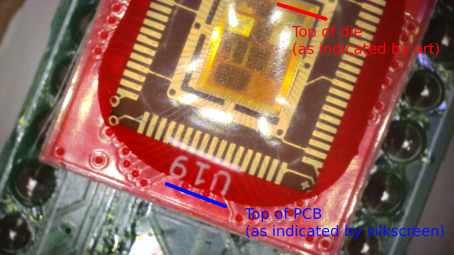
The dies are upside-down
🙀 3
2:49 p.m.
I don’t know what to do now
2:50 p.m.
Even if this is fixable by revision of the PCBs that the COBs plug in to, I have no money for that
2:50 p.m.
So its gonna be a couple months, at least
Avatar
afaik all remaining raw dies have been shipped out to me, so there is nothing that wafer.space can do on their end
2:59 p.m.
@Tim 'mithro' Ansell If you DO still have raw dies of mine, I would be willing to pay for another set of COBs with the die rotated correctly, as I am 100% sure that this would be cheaper than me re-designing and re-building all 8 PCBs I designed for this bring-up
3:01 p.m.
I am checking right now if the COBs as they are (flipped) are still usable
3:02 p.m.
Nope. They’re unusable. Power and ground are shorted to GPIOs all over the place. Most critically, two design select lines are shorted to ground, so can not be controlled. (edited)
3:03 p.m.
If I had made the locations of the power and ground pads symmetrical in my padring layout, I would still be able to bring up one or two things today with the generic DIP breakout, but as it stands, the COBs I have are bricks.
Avatar
Oh, the mosbius design on wafer space isn't public ? Can't find a link to the repo with gds and such ?
Avatar
Who was the other person that had custom COBs? They may wanna check theirs too.
Avatar
That's why I was asking about mosbius above.
4:49 p.m.
Althugh when they posted their COB design they did note QR code should be in the NE corner so that should be correct.
Avatar
Avatar
Tholin
Who was the other person that had custom COBs? They may wanna check theirs too.
Tim 'mithro' Ansell 2026-05-05 5:15 p.m.
I believe we have a bunch of your die still here at the bond house
5:21 p.m.
@Tholin - I believe we should be able to get another 20 bonded for you tomorrow. So now is the right time to discover that issue.
Avatar
Thank you
5:22 p.m.
The PCBs are fine, you just need to somehow instruct them to rotate the die 180°
Avatar
I wonder if a clear indicator of direction would help with preventing this in the future. Say, putting an arrow pointing outwards in one of the two remaining corners of the die, and a corresponding arrow pointing inwards on the PCB silkscreen? (edited)
5:43 p.m.
Actually, better idea. How would people feel about a script that reads in a padring configuration from a project and generates a KiCad symbol for it?
Avatar
Leo Moser (mole99) 2026-05-05 5:45 p.m.
Yes, we are planning some changes around how the corners are filled. @Andrew Wingate suggested keeping the corner opposite of the QR code empty to make the orientation more visible.
💜 1
Avatar
Avatar
Tholin
Actually, better idea. How would people feel about a script that reads in a padring configuration from a project and generates a KiCad symbol for it?
Leo Moser (mole99) 2026-05-05 5:45 p.m.
That would be great :) We could even integrate it into the precheck.
Avatar
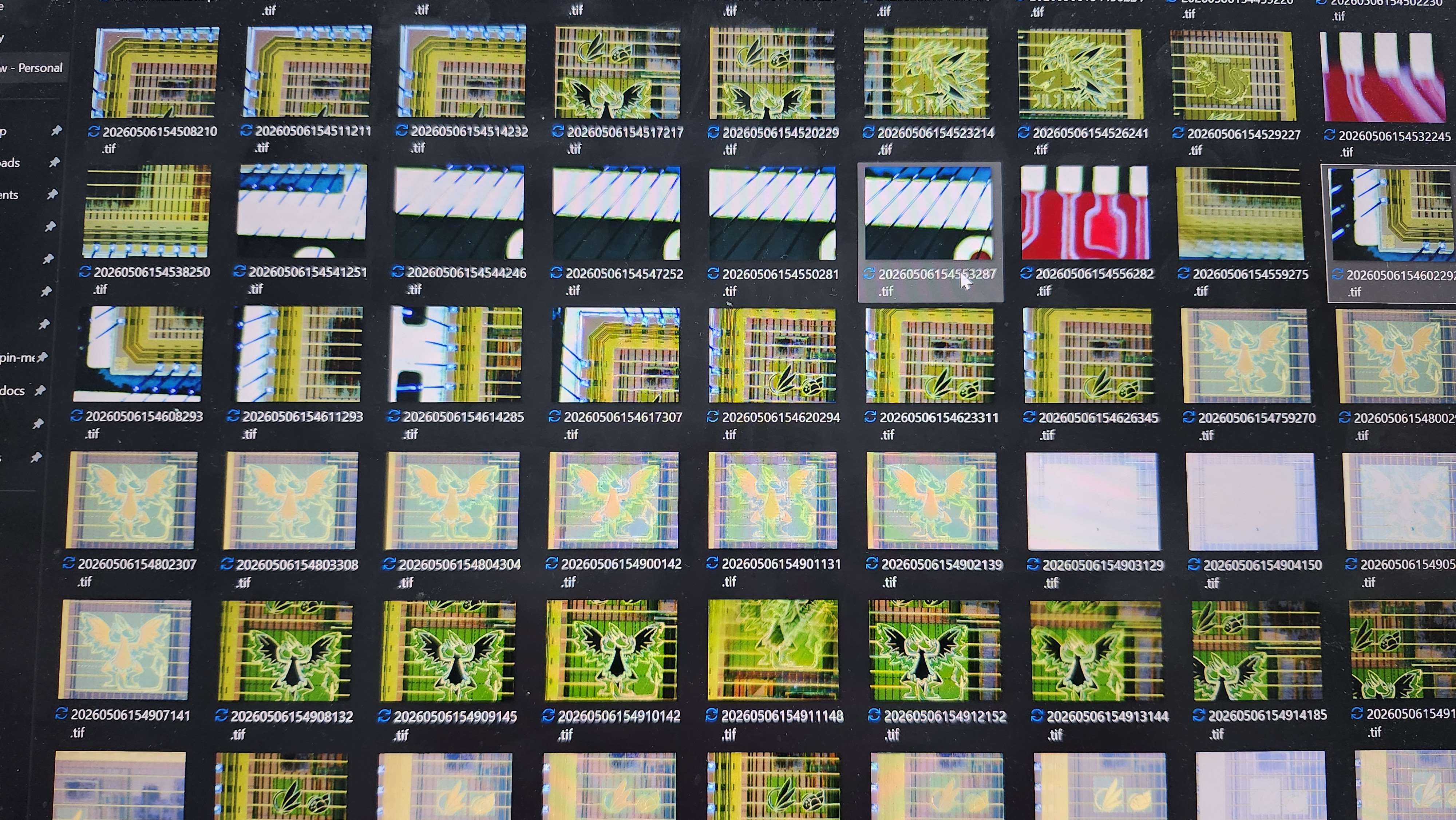
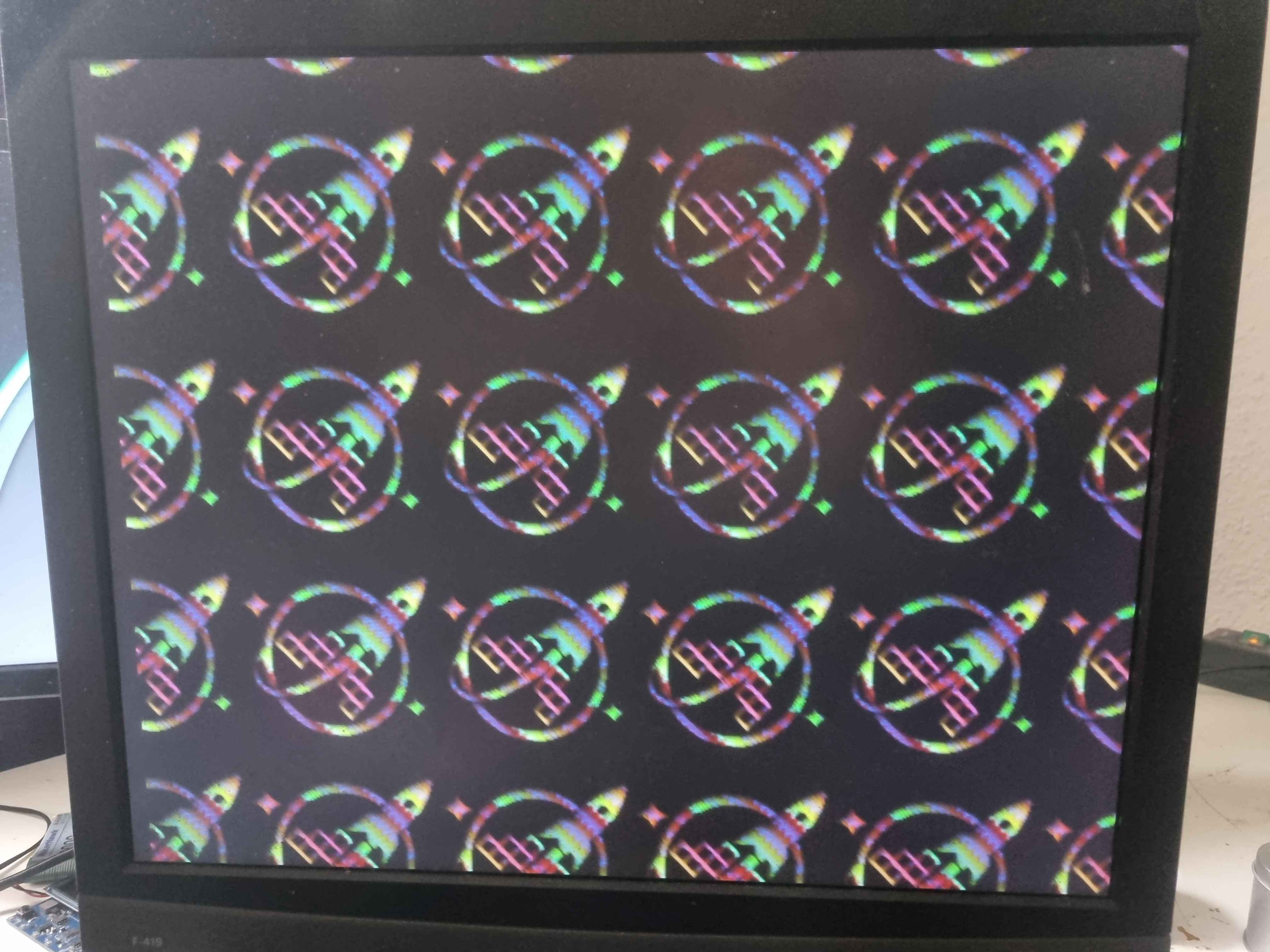
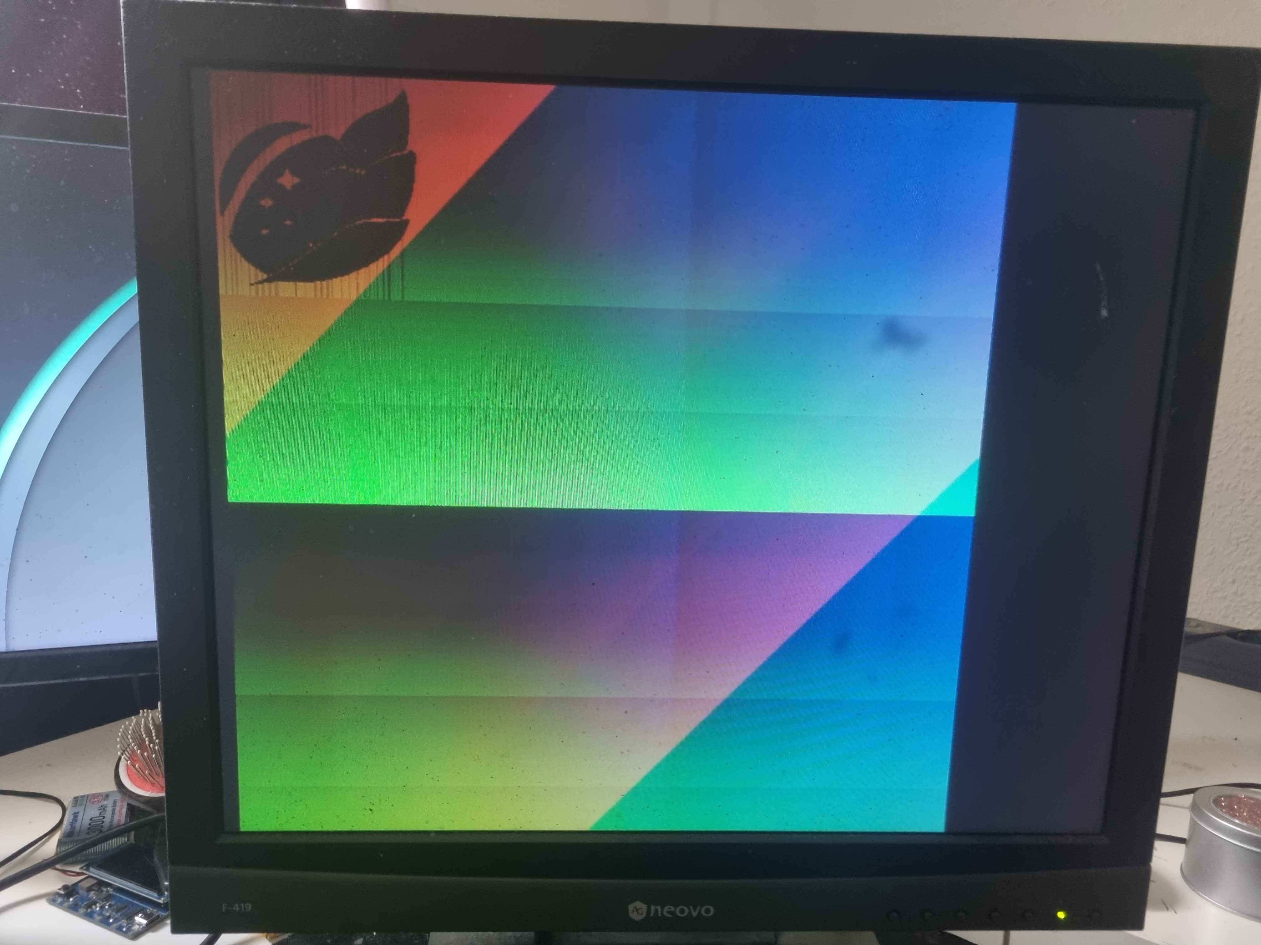
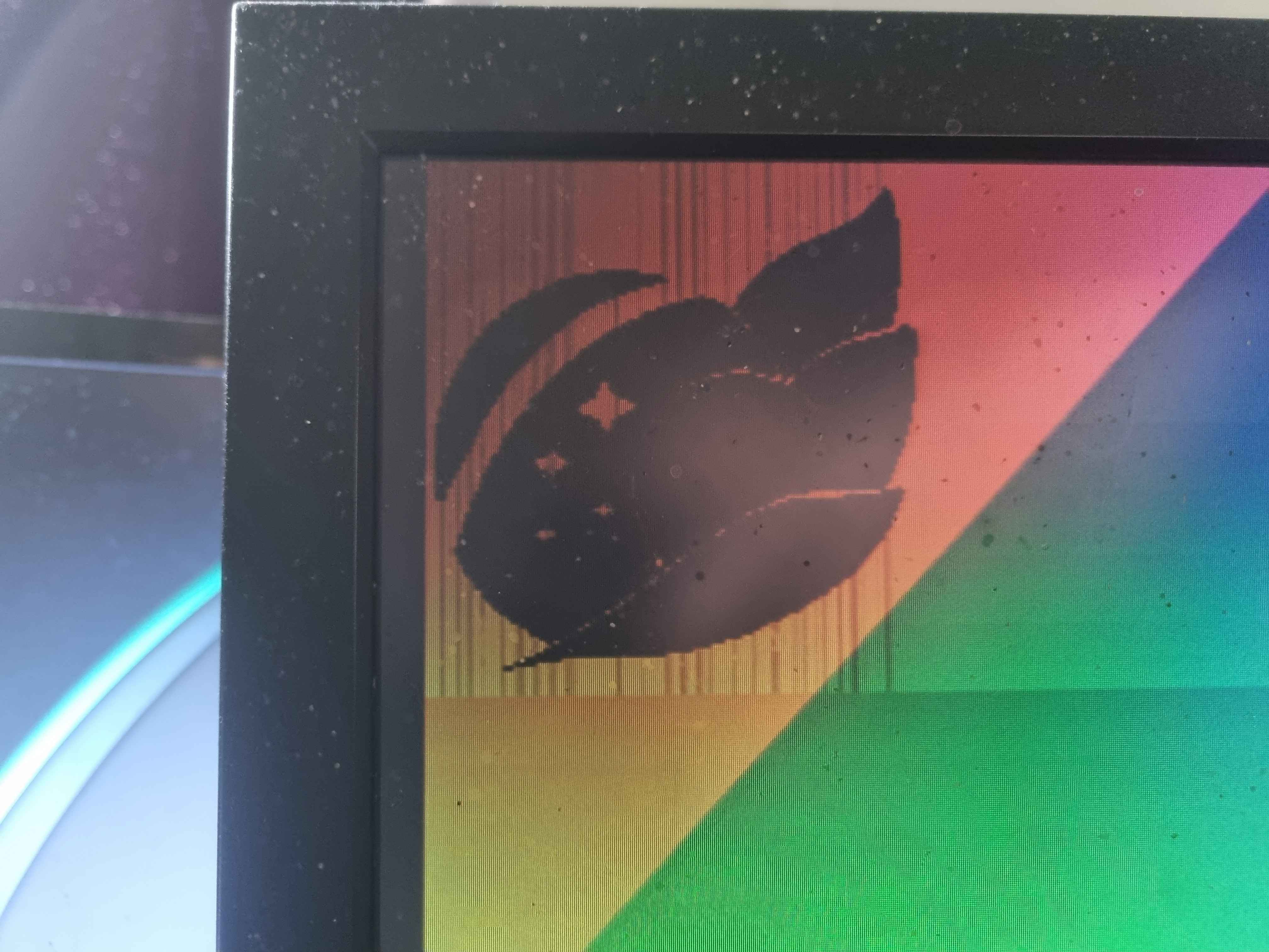
One thing I eventually want to work on (no promises when) is a 3D renderer that produces images of a die as it would appear under a microscope. I don’t think I can model all the quantum effects accurately, but I can approximate how things look specifically for gf180mcu.
👌 1
5:58 p.m.
I realized I’m maybe the only person in here with practical experience with multiple 3D rendering techniques, so I’ve added this to my todo list.
Avatar
Avatar
Tholin
I realized I’m maybe the only person in here with practical experience with multiple 3D rendering techniques, so I’ve added this to my todo list.
Andrew Wingate 2026-05-05 6:06 p.m.
I have been wanting to be able to make colorful images using refraction or other to generate the colors.
Avatar
I’m experimenting with it
6:07 p.m.
I’m preparing a layout that is just various dithering patterns in Metal5 and Metal4
💜 1
6:07 p.m.
To tape out on run2
6:07 p.m.
The amount of patterns I can do is limited due to DRC
Avatar
Andrew Wingate 2026-05-05 6:17 p.m.
Can't wait to see. Also Tim and I just landed in china. Tomoorw we will be visiting the bondhouse and believe you have more boards and die there @Tholin
Avatar
I got this cool photo, at least
👍 1
😎 1
Avatar
Could you still check bonding success rate checking for ESD diodes on the pins that are not shorted to GND/PWR.
Avatar
Tim 'mithro' Ansell 2026-05-06 7:53 a.m.
@Tholin - your die are being inspected by @Andrew Wingate and @Lauri
Avatar
Andrew Wingate 2026-05-06 7:54 a.m.
❤️ 5
Avatar
Tim 'mithro' Ansell 2026-05-06 7:54 a.m.
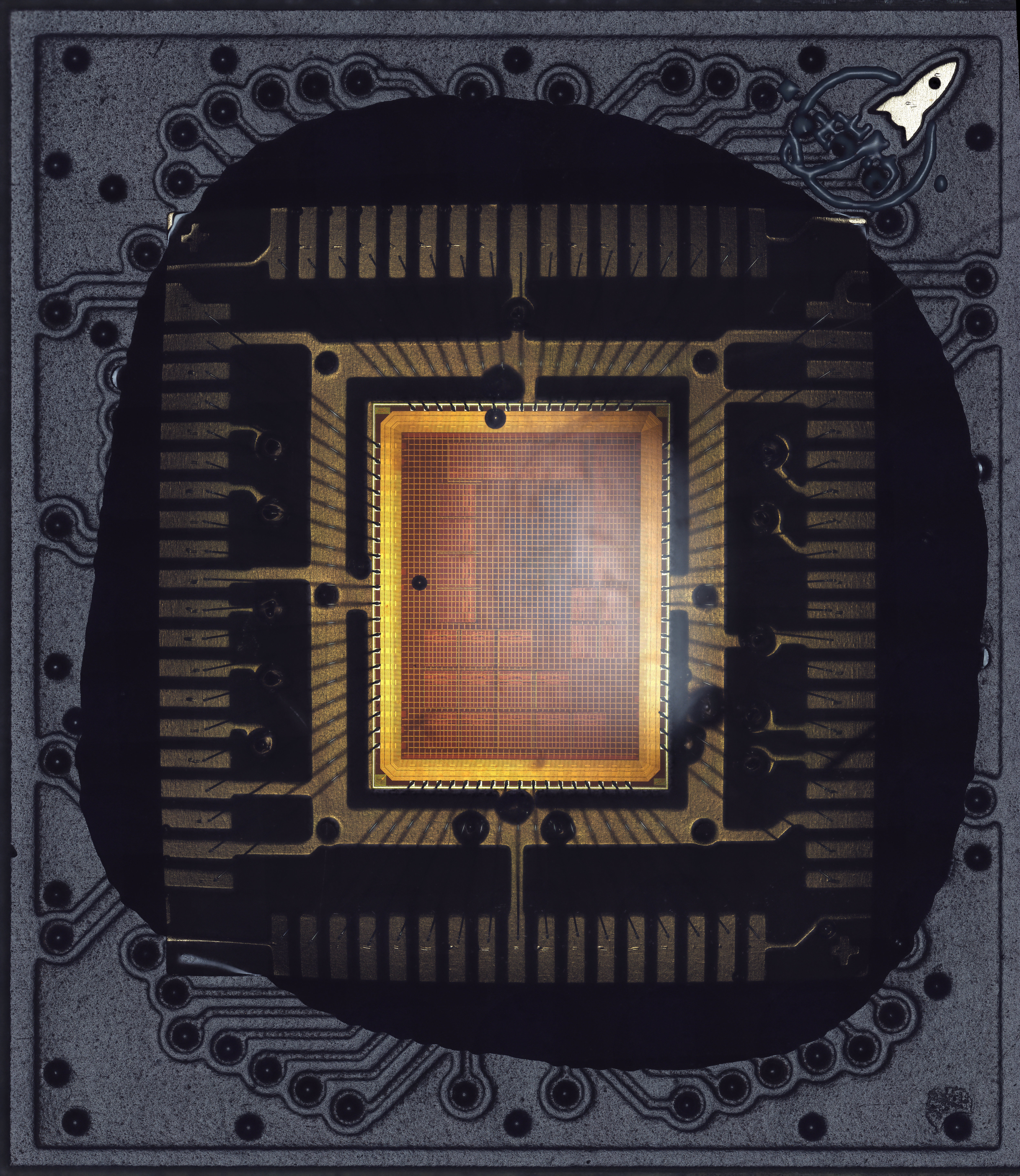
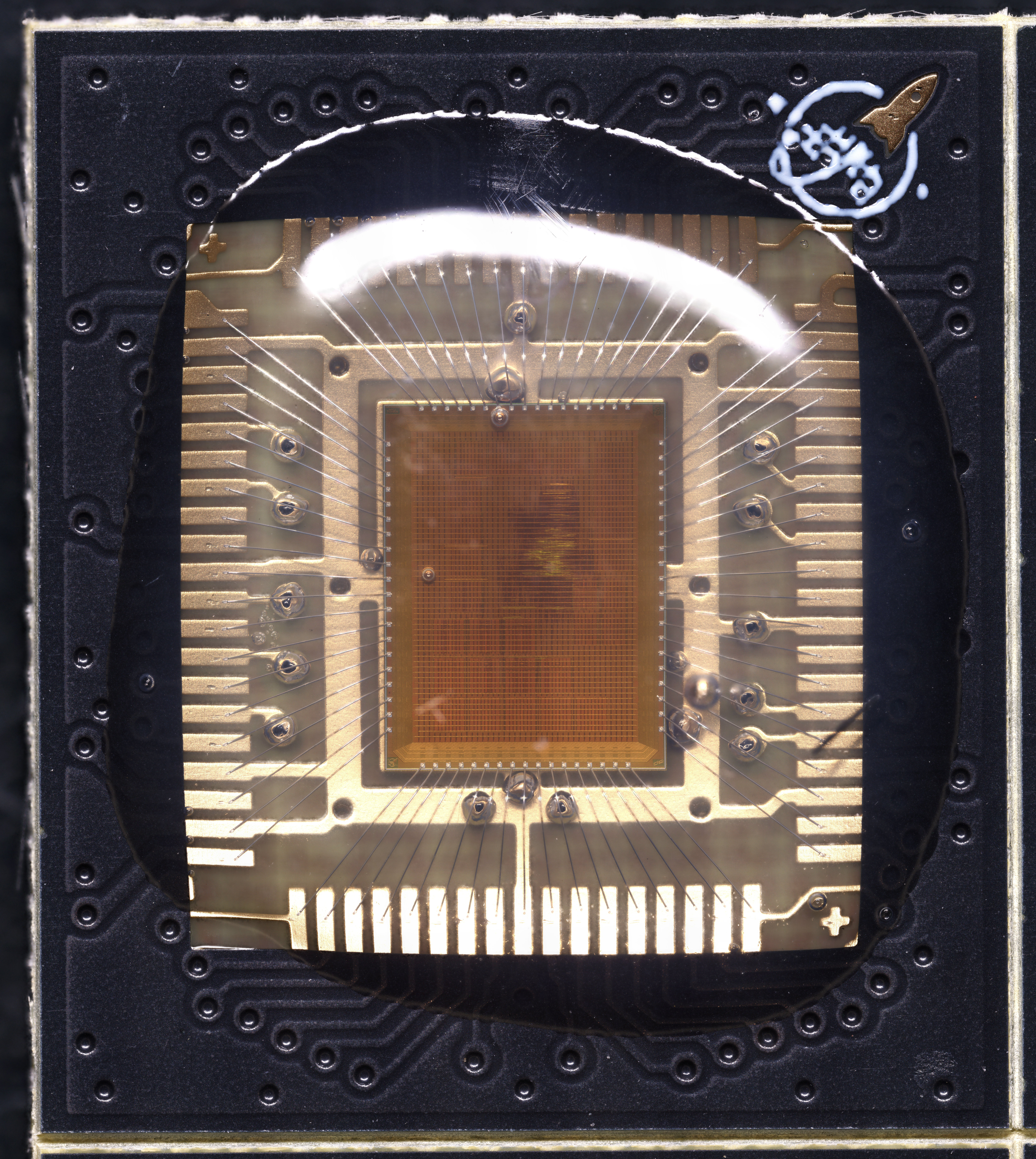
@Tholin - they are going to have like a couple 100mbs of photos of the die under different lighting and magnification for you.
Avatar
Andrew Wingate 2026-05-06 7:54 a.m.
Laptop cannot connect to discord from china
7:54 a.m.
*GBs
8:14 a.m.
That is going to be incredibly helpful
Avatar
Tim 'mithro' Ansell 2026-05-06 10:42 a.m.
The verification of Tiny Tapeout GF0p2 projects can be seen at https://tinytapeout.com/chips/silicon-proven/#ttgf0p2
Tiny Tapeout projects that have been taped out and verified in silicon.
Avatar
Tim 'mithro' Ansell 2026-05-06 10:49 p.m.
@Tholin - Still working with @Andrew Wingate to figure out how to upload the photos somewhere.
Avatar
How much is the total filesize combined?
Avatar
Tim 'mithro' Ansell 2026-05-06 10:59 p.m.
@Tholin - I think about ~35G (but that includes other die captures too).
Avatar
Ah, I see the problem
Avatar
Avatar
Tim 'mithro' Ansell
@Tholin - I think about ~35G (but that includes other die captures too).
Make a torrent? Unless you have need for access restrictions, that is.
Avatar
Avatar
namibj
Make a torrent? Unless you have need for access restrictions, that is.
Tim 'mithro' Ansell 2026-05-06 11:53 p.m.
I think a random torrent is likely to have more issues with hotel WiFi and China internet than just using rsync to put them on a server I have.
11:55 p.m.
Has anyone done simulation using the noise models in the GF180MCU PDK? If so, could you add any info you have to the thread @ https://discord.com/channels/1361349522684510449/1501344740350758992
Avatar
Tim 'mithro' Ansell 2026-05-10 2:20 a.m.
🎉 1
2:20 a.m.
So what can I do to get Zeptobars doing wafer.space silicon? 😛
Avatar
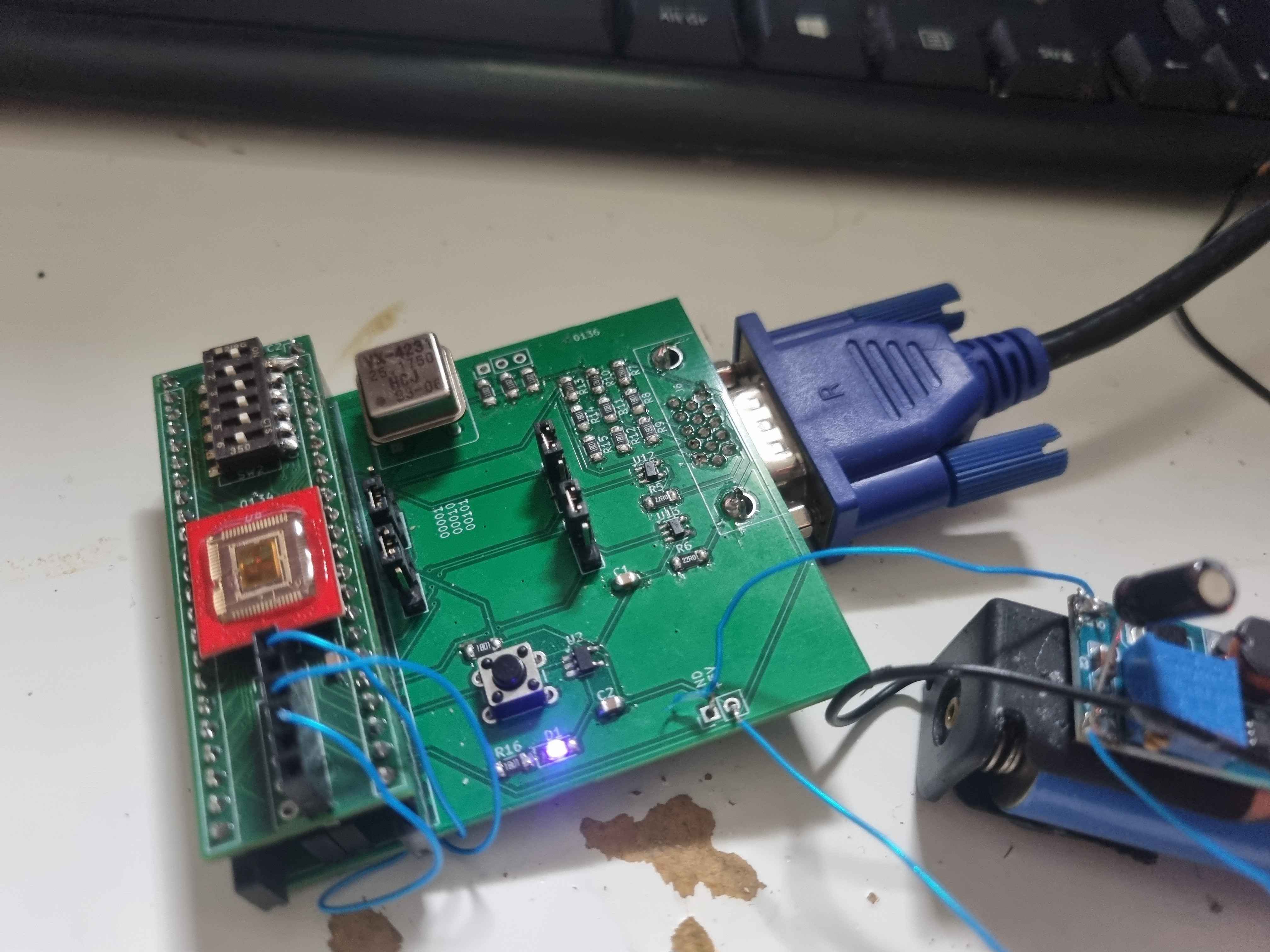
The wafer.space gf180mcuD JKU multi-project chip is alive! 🥳 Last night, I wired up the DIP adapter PCB on a breadboard. I just supplied the board with 3V3 or 5V via decoupling capacitors, connected my AWG to the clock input and tied the reset input to high... and voila, the sanity bring-up test works. On one digital output, the Super Mario Bros. theme song is played via a buzzer through a PWM signal. 🙌 Nothing fancy, just a quick breadboard build-up and test, but at least we can say that the chip is alive! 🎉 Next, our students can come in and test their own projects. Some motivated students have also decided to build a PCB as part of a seminar work. 🙌 I will also try to pour some dies into epoxy cubers. I have already received the materials for it. I just need to find some time for it. 🙂
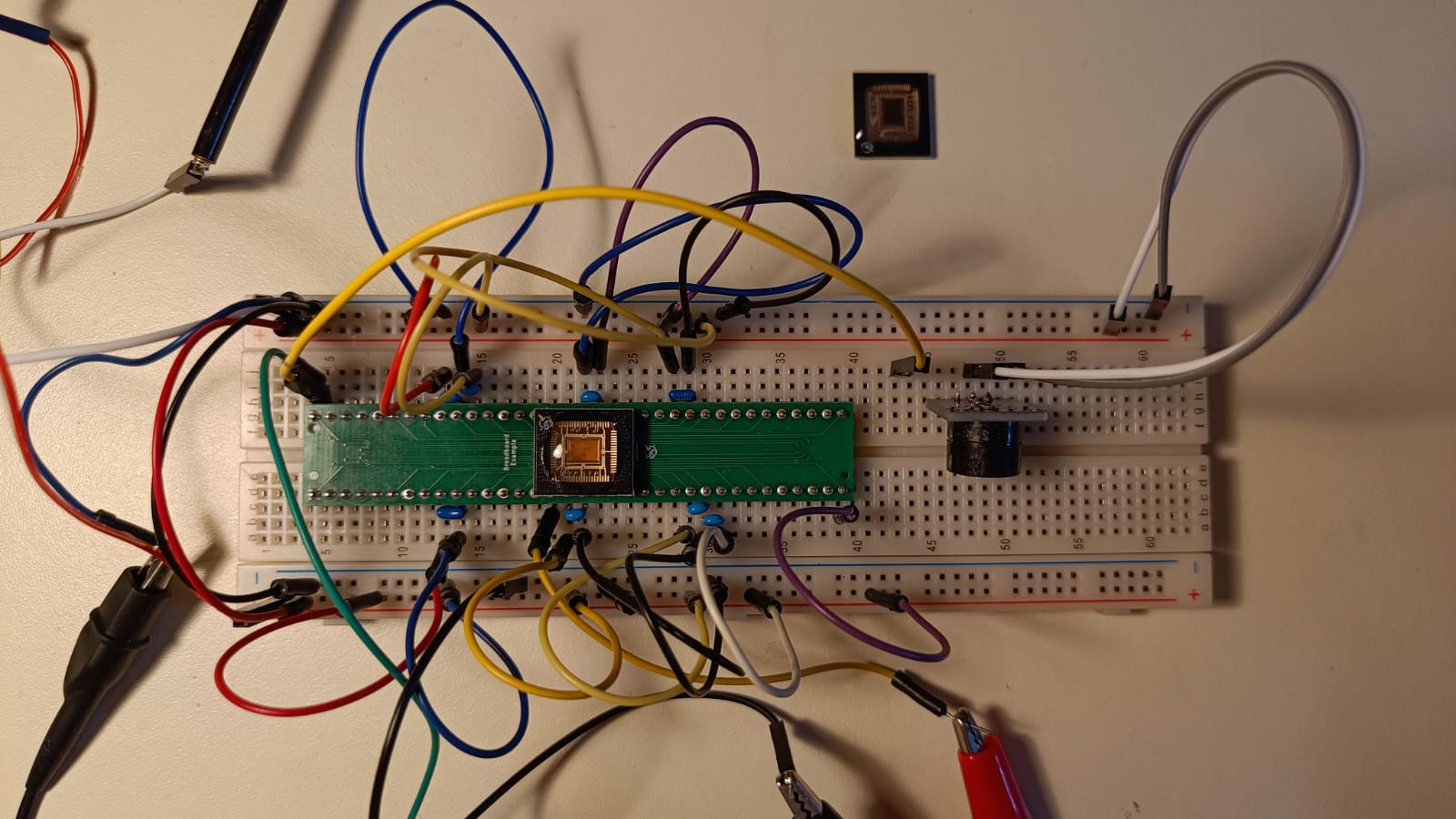
🎉 4
🥳 1
Leo Moser (mole99) started a thread. 2026-05-10 9:38 a.m.
Avatar
Avatar
Simi
The wafer.space gf180mcuD JKU multi-project chip is alive! 🥳 Last night, I wired up the DIP adapter PCB on a breadboard. I just supplied the board with 3V3 or 5V via decoupling capacitors, connected my AWG to the clock input and tied the reset input to high... and voila, the sanity bring-up test works. On one digital output, the Super Mario Bros. theme song is played via a buzzer through a PWM signal. 🙌 Nothing fancy, just a quick breadboard build-up and test, but at least we can say that the chip is alive! 🎉 Next, our students can come in and test their own projects. Some motivated students have also decided to build a PCB as part of a seminar work. 🙌 I will also try to pour some dies into epoxy cubers. I have already received the materials for it. I just need to find some time for it. 🙂
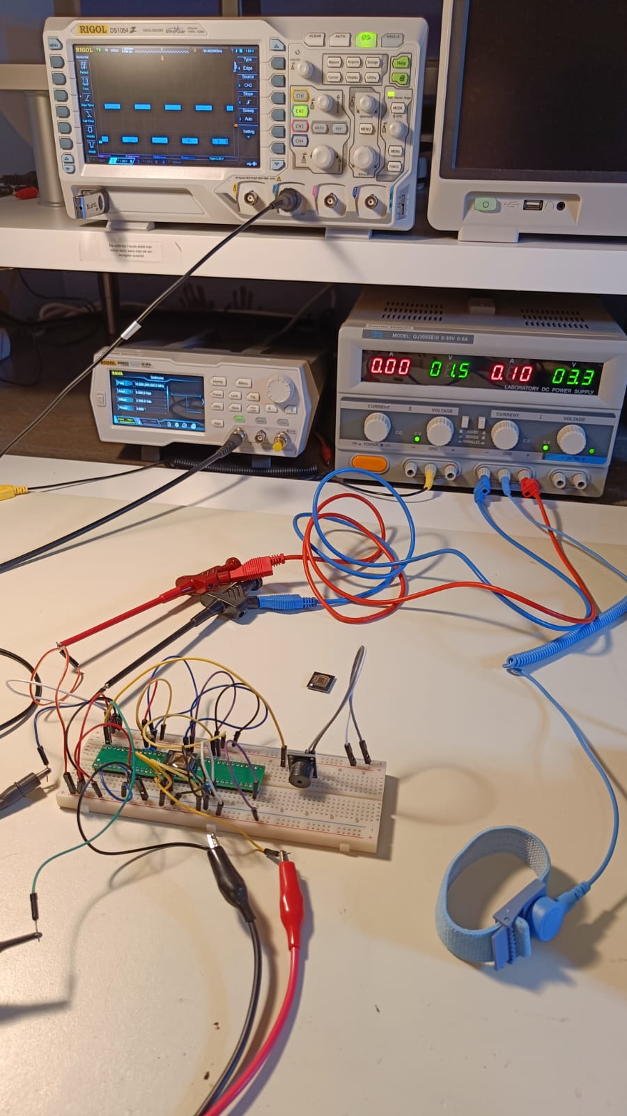
Tim 'mithro' Ansell 2026-05-10 10:27 a.m.
That is very cool!
🙌 2
Avatar
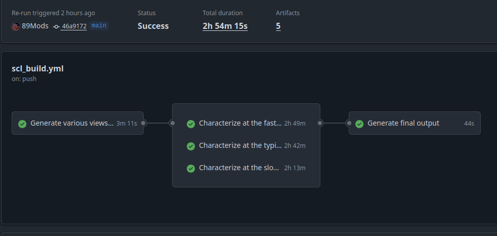
I’ve characterized my SCL at the ss_125C_3v00 corner, so all three corners are now done
👏 3
1:33 p.m.
I’m thinking of doing a 4th characterization at ss_080C_3v10 since that default slowest corner is kindof extreme. I don’t think anybody here needs their chips to be running at 125°C, so I’d like to offer an alternative maximum constraint of "just" 80°C at 3.1V
1:34 p.m.
So people can aim for a higher fmax at the tradeoff of a more constrained temperature and voltage range that the part is speced for.
1:35 p.m.
(I’m pretty sure at 125°C you start having other problems, like the epoxy on the COB melting)
Avatar
Avatar
Tholin
I’ve characterized my SCL at the ss_125C_3v00 corner, so all three corners are now done
Egor Lukyanchenko 2026-05-11 10:53 a.m.
Hi, @Tholin! Thanks for your amazing work on 3.3V SCL! Do you plan to extend your library? Because if you do, I would like to ask you to add some kind of delay cell to improve hold fixing. Currently I have problems with increasing a hold margin for my Caravel port, which I would like to do for safety. OpenROAD generates thousands of buffer cells but with only ~100ps delay each it has a hard time and takes a huge area.
Avatar
I’m currently working on making it easier for people to collaborate to the repo
12:40 p.m.
I’m just one person, unfortunately
Avatar
Avatar
Egor Lukyanchenko
Hi, @Tholin! Thanks for your amazing work on 3.3V SCL! Do you plan to extend your library? Because if you do, I would like to ask you to add some kind of delay cell to improve hold fixing. Currently I have problems with increasing a hold margin for my Caravel port, which I would like to do for safety. OpenROAD generates thousands of buffer cells but with only ~100ps delay each it has a hard time and takes a huge area.
Leo Moser (mole99) 2026-05-11 12:48 p.m.
A delay buffer appears to be simply two buffers in a trench coat, where the first three inverters have a narrow gate width. You might even want to experiment with the gate length for even larger delays. See here: https://gf180mcu-pdk.readthedocs.io/en/latest/digital/standard_cells/gf180mcu_fd_sc_mcu7t5v0/cells/dlya/gf180mcu_fd_sc_mcu7t5v0__dlya_1.html Adjusting Tholin's buffers would probably be a good start.
👍 1
Avatar
Building SCL releases is now fully automated
🎉 5
3:49 p.m.
3:50 p.m.
Just need to figure out how to actually generated repo releases from the actions output
3:50 p.m.
Stretch goal: verify the SCL by building an example project as part of the pipeline
3:50 p.m.
Currently blocked by LVS still locking up with the SCL
Avatar
so help me out here... can I build an octocore 6502 with 64b addressing?
10:22 p.m.
will that work here?
10:22 p.m.
or similar 'weird stuff'?
Avatar
the limitations are your imagination and silicon area
10:26 p.m.
well that and money to pay to a slot on the shuttle
10:27 p.m.
Complete 6502 CPU with bus multiplexer, GPIO, Timer, and UART
Avatar
ok, so im only limited by pads (pins) and available 'cells'/transistors?
Avatar
yeah pretty much
Avatar
Avatar
m_w
someone implemented 6502 on tinytapeout: https://tinytapeout.com/chips/ttihp26a/tt_um_chrismoos_6502_mcu
aye, I was talking to those guys, speed is limited to ~33mhz and a small number of pins
Avatar
that and the knowhow to implement all of the things
Avatar
i need 80-120 pins, and want to hit 800-1200mhz
Avatar
I think the pad ring is not that big
Avatar
it said 56-120+ pads
10:30 p.m.
on the website, so im not sure if we mean different things, perhaps some are multiplexed
Avatar
yeah the default isn't that big
Avatar
im not sure yet
10:30 p.m.
just getting some conceptual boundaries
Avatar
you are on your own if you don't use the default
Avatar
ok, 'can I make the whole thing SRAM'?
Avatar
how many 'cells'?
10:31 p.m.
or transistors do i get?
Avatar
depends on a lot of things
10:34 p.m.
@Tim 'mithro' Ansell or @tnt might have some approximate numbers
Avatar
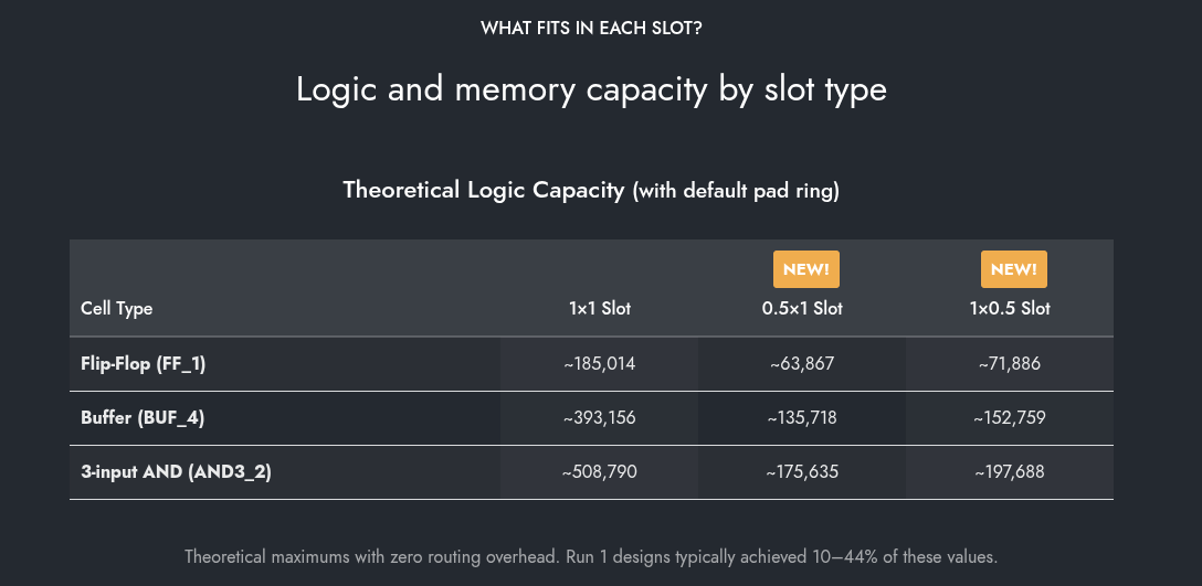
there's some information here total cells used/% area used: https://github.com/wafer-space/ws-run1/blob/density-report/reticle_density_report.md
wafer.space GF180MCU Run 1. Contribute to wafer-space/ws-run1 development by creating an account on GitHub.
Avatar
TIny Tapeout projects also show the number of cells used in the GDS github action
Avatar
Here's mine as an example for Tiny Tapeout https://github.com/FangameEmpire/ttsky26a_spacewar/actions/runs/25696603247 2200 cells ~= 70% of two tiles (edited)
A scaled-down version of the classic PDP-1 game on a VGA display. - Merge bullet tests back into main · FangameEmpire/ttsky26a_spacewar@f151f17
10:40 p.m.
Or do you mean wafer.space as a whole
Avatar
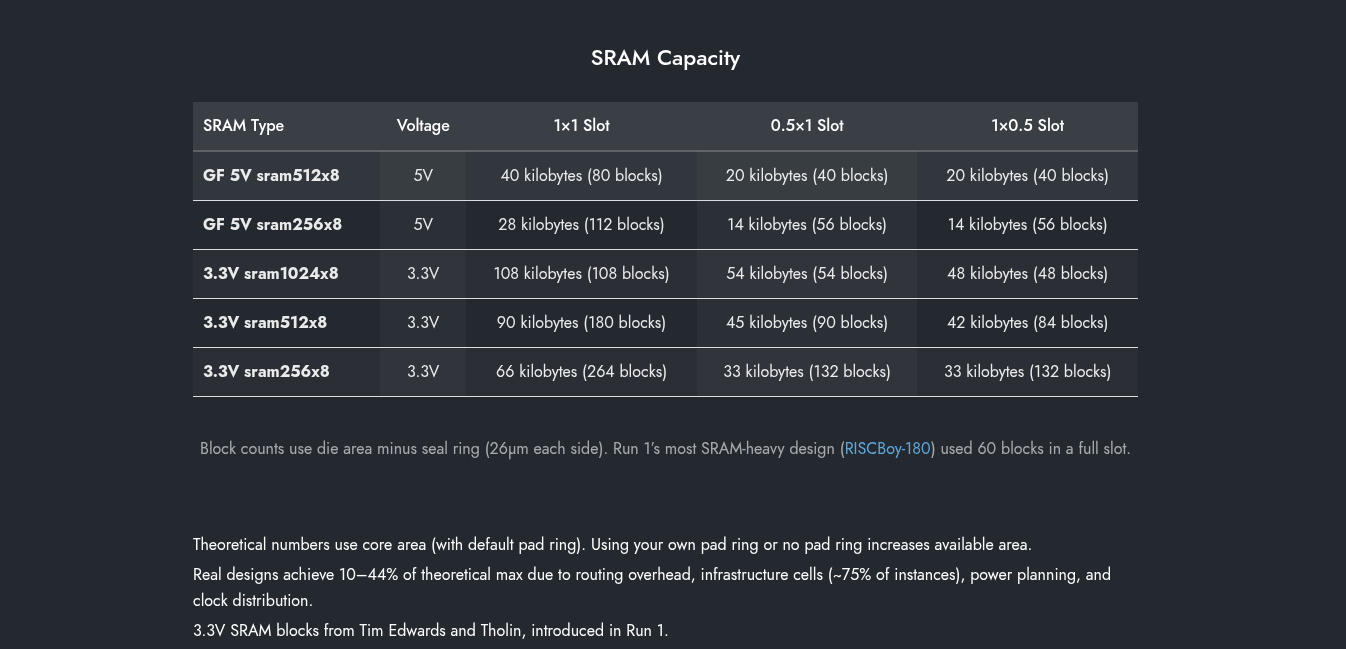
all of this is on the main page
Avatar
Avatar
m_w
Click to see attachment 🖼️
Read the little text down below
10:44 p.m.
Those are theoretical, using the standard cells included in the temolate
Avatar
not sure what you are expecting?
Avatar
Oh sorry I am very sleepy and thought you were wayfarer
10:45 p.m.
Wow I really need either new glasses or a few more than eight hours of sleep
10:45 p.m.
Again really sorry
Avatar
it is fine just giving the basic idea
Avatar
looks like its fine for some basic ideas. creating a large sram array with embedded processor is not trivial however
10:47 p.m.
i wasnt sure if the SRAM listed was 'if its all ram' or in addition to some other components
10:48 p.m.
i have some 65xx variations/other architectures im interested in developing, including ML algorithms in vhdl
Avatar
yeah those are estimates based on the area of a cell and the user area
Avatar
an octocore 6502 that can chain handle 64b is certainly a goal, as is some math coprocessor for 6502/816 etc
Avatar
since the tools are free you can run some experiments and get an idea of what you can do
Avatar
i even have a 4bit 6404 microslice design i might test out someday, as well as a coprocessor for the 6502 that increases address space and some other functions
10:51 p.m.
i mean, im starting on an fpga, i have some ideas for a hardware company and might try to build some custom stuff, presales/crowdsourcing etc to get funded
Avatar
does a 'smart digital drawing tablet/e-reader' need a 64bit cpu? what if it uses expired patents from the wacom intuous2 line?
Avatar
Avatar
Wayfarer
does a 'smart digital drawing tablet/e-reader' need a 64bit cpu? what if it uses expired patents from the wacom intuous2 line?
probably not. not a lawyer. 🙂
Avatar
well, not a legal question, more a theoritical one
11:01 p.m.
there are some cool devices well served by simple hardware
Avatar
yes it could probably work on a 8 bit processor 🙂
Avatar
now wafer.space just burns the silicon, it has to go to packaging afterwards?
Avatar
well it does wire bonding to COB if you pay a little extra
11:06 p.m.
but yeah it is a very minimal process
11:07 p.m.
notice the cost 🙂
11:09 p.m.
I think if you want QFN then chipfoundary might be easier path https://chipfoundry.io/
ChipFoundry
Avatar
it will all depend on time, energy and money
11:14 p.m.
they want 15K usd
Avatar
yeah it is a newer process and packaging is not cheap (edited)
Avatar
Avatar
m_w
yeah it is a newer process and packaging is not cheap (edited)
Unless I forgot, they are (almost?) stricter on the pad ring than the WS COB seems to be, and packaging is not anywhere near 150$/QFN.
Avatar
i mean, if i have volume its probably worth it, though they seem big around risc-v
Avatar
(IIRC they run the entire lot through the same packaging and just make sure they know afterwards which of the designs that share the reticle ended up in the particular QFN, such that they can keep them sorted.)
Avatar
Avatar
Wayfarer
i mean, if i have volume its probably worth it, though they seem big around risc-v
WS is comparatively affordable. iirc the early bird pricing was 4$/chip @ 1k
11:36 p.m.
iiuc that assumes packaged via COB onto the mezzazine socketable package/board and the standard pad ring.
Avatar
yeah this is way cheaper
11:39 p.m.
per chip
Avatar
like, maybe i can explain... I dream of owning an electronics company. and building ruggedized electronics for hobbyists, education, farmers, truckers and the trade industry... games and art stuff. my mom has this little "50-in-1" color video game on the back of the bathroom door. it plays pong and a racecar game and checkers and such... its like, 8bit. you can buy these a dime a dozen on 'the bay' or 'the rainforest (amazon)' none are made i America. I want to be the guy with an American factory that makes these, and e-readers, trail computers, gps, digital logbooks for truckers, a nice 16b drawing tablet. a retro console you can hook up to modern tvs, construction site computers, AR/VR headsets, etc. "I wanna be the guy" ... who picks red or blue, and makes jobs for some really talented people, while building hardware and software I think it cool.
11:40 p.m.
so, if this is a step towards that, I still have years until Im retirement age
11:40 p.m.
and Ill probably want to run this company long after that (edited)
11:41 p.m.
im ok, not being the biggest, most profitable. I like open hardware design.
11:41 p.m.
its going to take 'economy of scale' for any of it to work out at all
11:42 p.m.
i probably should have gone for an MBA in finance huh?
Avatar
Avatar
Wayfarer
like, maybe i can explain... I dream of owning an electronics company. and building ruggedized electronics for hobbyists, education, farmers, truckers and the trade industry... games and art stuff. my mom has this little "50-in-1" color video game on the back of the bathroom door. it plays pong and a racecar game and checkers and such... its like, 8bit. you can buy these a dime a dozen on 'the bay' or 'the rainforest (amazon)' none are made i America. I want to be the guy with an American factory that makes these, and e-readers, trail computers, gps, digital logbooks for truckers, a nice 16b drawing tablet. a retro console you can hook up to modern tvs, construction site computers, AR/VR headsets, etc. "I wanna be the guy" ... who picks red or blue, and makes jobs for some really talented people, while building hardware and software I think it cool.
ambitious..... like, a lot.
Avatar
yeah, so i want to start small, with some open hardware designs and sell kits
11:56 p.m.
i have a masters in instructional design and technology, I was a year away from a phd in computer engineering when my advisor retired
11:57 p.m.
im published on a paper about technical risk, the project was a simple 6502 based computer kit for education
11:57 p.m.
i plan to open source the design and try to market it to schools, colleges etc, hobbyists
11:58 p.m.
i have the parts for the prototype on my desk over there
11:58 p.m.
its <$100 usd, and has a lot of support on the 6502 forums
11:59 p.m.
beyond this, I want to improve the design to Mk2, and see if I can get it to function as a good calculator/solver
11:59 p.m.
maybe, in the next 2 years
Avatar
Avatar
Wayfarer
like, maybe i can explain... I dream of owning an electronics company. and building ruggedized electronics for hobbyists, education, farmers, truckers and the trade industry... games and art stuff. my mom has this little "50-in-1" color video game on the back of the bathroom door. it plays pong and a racecar game and checkers and such... its like, 8bit. you can buy these a dime a dozen on 'the bay' or 'the rainforest (amazon)' none are made i America. I want to be the guy with an American factory that makes these, and e-readers, trail computers, gps, digital logbooks for truckers, a nice 16b drawing tablet. a retro console you can hook up to modern tvs, construction site computers, AR/VR headsets, etc. "I wanna be the guy" ... who picks red or blue, and makes jobs for some really talented people, while building hardware and software I think it cool.
id recommend studying a bit of economics and maybe doing an online business course if you're dead set on this idea
12:00 a.m.
there are many reasons why things aren't all made in the US, most of them benefit the US more broadly
Avatar
Avatar
Christopher
id recommend studying a bit of economics and maybe doing an online business course if you're dead set on this idea
yeah indeed. I have an incomplete in markov processes and I just got into a grad certificate program in nuclear nonproliferation to keep status as a degree seeking student
Avatar
Avatar
Christopher
there are many reasons why things aren't all made in the US, most of them benefit the US more broadly
so many people need jobs, and education is really lacking here, Im hoping to address both concerns
Avatar
well, you're not going to address both concerns without first knowing the stomping ground yourself
Avatar
if I will accept 'not making millions per year personally', I think I can stay competitive
Avatar
Avatar
Wayfarer
if I will accept 'not making millions per year personally', I think I can stay competitive
thats not really how this work
Avatar
Avatar
Christopher
well, you're not going to address both concerns without first knowing the stomping ground yourself
yeah my bachelors is interdisciplinary studies, I took a lot of business courses in grad school too, mostly management though... I collect books and recently got a bunch of stuff on economics.. MIT opencourseware might be a good place to look for classes
Avatar
Avatar
Christopher
thats not really how this work
its more an expression of humility, and acknowlegement that manufacturing is all but dead in the US. I thnk it could see a revival though, if Im willing to compete for market share instead of market dominance, I think ive got some disruptive ideas here
Avatar
you cant run a business without making profit
Avatar
though, maybe im just being optimistic. do you have a background in business?
Avatar
manufacturing fights for thin margins
ferristhumbsup 1
Avatar
well, a nonprofit is a business, profit is its own thing, Im not saying I want to run this business as a non profit, though low margins were more what I was thinking. you cant run a business without being solvent, Im aiming for solvency, profit would be great.
12:09 a.m.
for example, we quit making tvs in America some years ago. to understand why, is multifold, though comes down to profit margin, it was just way cheaper to make them in mexico and china, etc. these days india is surging ahead in manufacturing. environmental regulations, workplace safety, and employee expectations are all a factor. the thing I can change, is to reduce executive compensation, reduce greed, and focus on other things
12:09 a.m.
like, theres a guy, CEO, and instead of making millions a year, they make 70k like the rest of their managers
12:10 a.m.
im fine with that, if it creates a sustainable process
12:10 a.m.
yet I understand, my willingness to take a smaller check, is only one factor
12:10 a.m.
do you have much experience running or starting a business?
Avatar
Avatar
Wayfarer
for example, we quit making tvs in America some years ago. to understand why, is multifold, though comes down to profit margin, it was just way cheaper to make them in mexico and china, etc. these days india is surging ahead in manufacturing. environmental regulations, workplace safety, and employee expectations are all a factor. the thing I can change, is to reduce executive compensation, reduce greed, and focus on other things
india is surging in part because theyve been so impoverished for such a long time, and they're being massively impacted by gas shortages right now...
Avatar
awesome. Ive not done a lot of manufacturing. i have some grad certificates relating to entrepreneurship and innovation, though in life sciences, it was a lot of health device regulations, and a grad certificate in organization change and consulting, which is mostly management org psych. Ive run a small business off and on for decades, though mostly just me providing services to others, computer repair, web design and landscaping/lawn care a far cry from manufacturing electronics, though some stuff is practical experience. like I said I was a year off from a phd in computer engineering (my advisor retired for health reasons). i do what I can here and there.
12:43 a.m.
i would honestly say a few courses in finance/accounting would be very close to an MBA.
12:44 a.m.
ive got the management and regulatory stuff, just not the money side, nor a lot on manufacturing. selling crafts on a small scale yes, not making thousands of units per week or such
12:44 a.m.
now I do think if I move towards used equipment, niche markets and simple designs, I might do ok
12:45 a.m.
ive written a few business plans and work plans over the years. do you work in semiconductors?
Avatar
Tim 'mithro' Ansell 2026-05-12 6:59 a.m.
If you want open source semiconductors manufactured in the US, the ChipFoundry.io is your current only choice. wafer.space is a Singaporean company which provides access to silicon that is manufactured in Singapore by GF.
7:01 a.m.
If you want to build your own "budget silicon foundry" then you might want to check out the HackerFab group. They are doing some interesting stuff but it is more late 1980s / early 1990s level at the moment and definitely not cost competitive for anything in volume.
👍 2
Avatar
why open source? do you just mean open access? i have no problem using a company in singapore, Im not sure why thats important at some point, if I could get my own machines in house to do this in the US, it would be really cool.
Avatar
Pretty sure "open source" here means that you get access to a PDK without having to sign NDAs, and effectively getting married to the platform (edited)
Avatar
gotcha, ok. its just a different use of the jargon many of these platforms (small business fabrication) want you to use 'their chips' or 'their shell',, and using a template is helpful to some. I just happen to be looking for a place I can have specific control of what Im building
Avatar
Well, that also depends on what's in their PDK - which is also good if you can access it before signing a contract
Avatar
likem the ISAAC/ISAc,, its an ISA/AT-bus controller for small platforms, and it has specifc requirements, so finding a good fit is important
Avatar
Avatar
dshadoff
Well, that also depends on what's in their PDK - which is also good if you can access it before signing a contract
is that 'product development kit'?
3:24 p.m.
process design kit?
Avatar
Maybe more like "process". Not sure what it stands for exactly, but it's a definition of things like standard cells and all the nitty gritty that you would need in order to simulate
Avatar
right, so atm, to get started, today Im looking for a white label company to put my brand name on flashlights
Avatar
I'm not an expert on the space; just trying to answer a couple of the simpler questions.
Avatar
as I move forward, I have a couple of small devices that require unique silicon
Avatar
Avatar
dshadoff
I'm not an expert on the space; just trying to answer a couple of the simpler questions.
no totally, just a 'today I am', how Im trying to generate capital/revenue
3:30 p.m.
ISAAC is an 8b AT/ISA bus controller. it pairs with a 6502, an lcd driver (like an EVE or Epson SD chip), and similar chips plus we are looking for an audio driver/processor for a set of small handheld devices so Tiny Tapeout might be a good choice for that audio chip, they cant handle an ISA controller (not enough pins) their VGA experiments are rudimentary, and so wafer.space seems more our speed for a couple of these
3:31 p.m.
tiny tapeouot is 'very cool', they just dont have the 'oomph' in terms of capabilities for a lot of stuff. maybe for a 4bit microslice or 8b math coprocessor, etc wafer.space, seems 'bigger', though its 1000 'units' at $4000+
Avatar
TinyTapeout is just a multi-project-per-die system for getting onto multi-project wafers. I.e. the last wafer.space run also had a TinyTapeout as one of the projects. Think of it like a multi-board PCB house, and TinyTapeout is splitting one of the boards amongst friends who are all sharing the same physical PCB
3:34 p.m.
meaning the wafer.space and the tinytapeout projects that ran on GF180 had the same capabilities (made in the same fab etc), just different amount of silicon to work with
Avatar
ok gotcha, it just seems like they are more limited overall another place I looked required riscV in some manner. finding the right fabricator is certainly going to be an important step. I just dont want to get locked into 'building for a system and its constraints'
3:39 p.m.
so far, wafer.space seems to be 'the most open' or 'blank slate' I can find
Avatar
It will be more limited mainly because you're sharing silicon and pins with other projects, yes. If you are mostly in "digital" land, RTL (the programming language for hardware) is mostly portable. You can take the RTL for a RISC processor and tape it out on both Sky130 and GF180 (or TSMC 65 etc etc) without too much fuss. The trick is that most fabs require you to sign an NDA to get the process kit that lets you actually "synthesize" the transistors. So without that NDA, you're limited to the handful of open fabs like Sky130, GF180, and whatever the IHP one is That said, you're still going to have to build for a system in mind. I.e. older nodes aren't very efficient for SRAM so it ends up eating a ton of space and you're design will reflect that. Newer nodes are trickier with analog, etc etc
Avatar
so 'standard cells', is this like fpga LUTs? i see it thrown around, its ~4-20 transistors right?
Avatar
Avatar
BreakingTaps
It will be more limited mainly because you're sharing silicon and pins with other projects, yes. If you are mostly in "digital" land, RTL (the programming language for hardware) is mostly portable. You can take the RTL for a RISC processor and tape it out on both Sky130 and GF180 (or TSMC 65 etc etc) without too much fuss. The trick is that most fabs require you to sign an NDA to get the process kit that lets you actually "synthesize" the transistors. So without that NDA, you're limited to the handful of open fabs like Sky130, GF180, and whatever the IHP one is That said, you're still going to have to build for a system in mind. I.e. older nodes aren't very efficient for SRAM so it ends up eating a ton of space and you're design will reflect that. Newer nodes are trickier with analog, etc etc
im a vhdl guy, and yes, a lot of this is new jargon. i think i see what yo are saying though at least to some degree
Avatar
Avatar
Wayfarer
so 'standard cells', is this like fpga LUTs? i see it thrown around, its ~4-20 transistors right?
a "standard cell" will be basic components like AND, OR, NOT, NAND etc as well as things like buffers, inverters, delay cells, flip flops. You can see the full list here for gf180: https://gf180mcu-pdk.readthedocs.io/en/latest/digital/standard_cells/standard_cells.html But yeah each is like 3-10 transistors depending on complexity Your VHDL gets synthesized to this base list of standard cells, then OpenRoad (or proprietary software) places and routes connections to all those cells like a PCB autorouter
Avatar
ok, gotcha. so 'standard cell' ~= 'gate or feature'
Avatar
yep pretty much 🙂 so if you switch fabs, you get a new PDK with a new set of standard cells, but the synth -> place -> route process is mostly automated. Hit recompile and essentially rebuild the same logic on a new fab process
Avatar
how many cells do i get for a 1x1 die?
Avatar
scroll down to "Theoretical maximum standard cell density" on the wafer.space website and Tim has some numbers, as well as real numbers from the first Run
3:49 p.m.
most dense real design was ~316k logic cells it looks like
Avatar
i found it, so it will vary based on routing/complexity
Avatar
yep!
Avatar
im getting '100k cells average' at a glance, more if you are optimized, maybe 150k
3:51 p.m.
so it is certainly realistic to consider "an 8 core 6502, that has a 64b mode" or similar levels of complexity.... you could put an 80386 on here ok
3:52 p.m.
i think this is probably a good fit for me in the long run, once I have a more concrete design.
Avatar
couldn't say, outside my experience 🙂 but someone taped out a Z80, and iirc the 6502 was a really old fab node (like 10um or something?) so probably very doable. For me at least, the biggest hurdle was just SRAM size because I didn't want to deal with off-chip flash. there's gobs of space if you're just doing digital logic without much need for memory

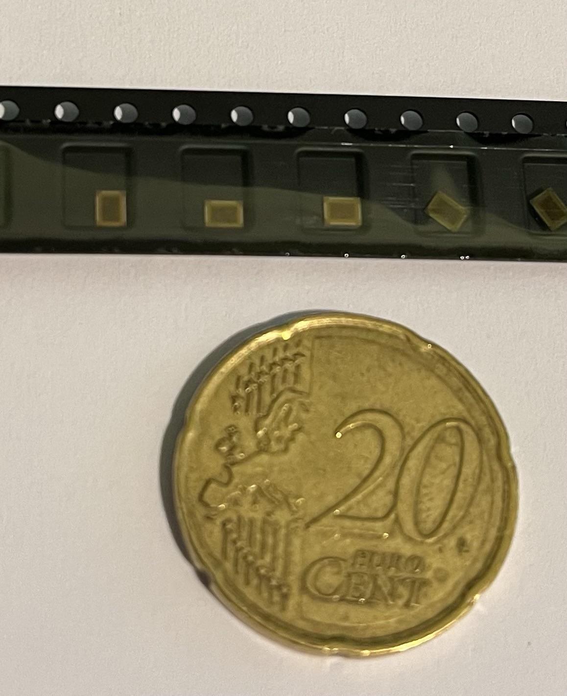
3:56 p.m.
(work time, bbl!)
Avatar
yeah 6502 had no on chip ram, though adding some is certainly a goal
Avatar
Avatar
BreakingTaps
(work time, bbl!)
have a good day, Im hunting drop shipping suppliers here for some working money
Avatar
Avatar
Wayfarer
yeah 6502 had no on chip ram, though adding some is certainly a goal
Well, also keep in mind that 6502 was NMOS, not CMOS - everything nowadays is CMOS. But wafer.space does have 5V logic standard cells available.
4:06 p.m.
(I expect most places would concentrate on 3.3V logic and I/Os)
Avatar
65c02 and 65ce02 were cmos
4:06 p.m.
they still make the 65c02 today
4:06 p.m.
iu just want custom chips
4:07 p.m.
i should say '6502 based'
Avatar
Yes, I'm just mentioning it in case you were planning on making a plug-in replacement, threshold levels and so on would need to be considered
Avatar
no, im more looking at the ce02 variant and going my own direction while maintaing the overall Instruction Set
4:08 p.m.
6509 is a cool design, it had more memory/address space and better conforms to the AT bus
4:09 p.m.
i have a portable 8b game platform that can plug into a tv and upscale from 480x270 or so to fHD built for the 8b style of games. marketed at hobbyists, enthusiasts etc
4:10 p.m.
it needs either a 'full 6502 based SoC', or the ISAAC I mentioned and such
4:11 p.m.
im almost certain if I could fab out some 6502s (based systems) with onboard ram and better i/o I could sell a few thousand, its just getting everything lined up
4:11 p.m.
beyond these designs, Im looking at ML algorithms implemented in hardware, in-memory and near-memory computing etc
4:12 p.m.
6502 stuff is my playground though, how Ill learn the basics
Avatar
I finally got back to collect my bare dies! The quarter slot ones are very small. https://hachyderm.io/@rebelmike/116563528101924895
Attached: 1 image I received some silicon from wafer space run 1! These are just for display purposes - we’re still working on getting a board together to allow some to be bonded. But they are a version of my TinyQV SoC in a “quarter size” wafer space slot.
👍 2
🎉 1
Avatar
Avatar
RebelMike
I finally got back to collect my bare dies! The quarter slot ones are very small. https://hachyderm.io/@rebelmike/116563528101924895
those look so small you could accidentally inhale one
Avatar
Yes, they are tiny!
Avatar
Update: the dies are right side up this time
🎉 4
2:24 p.m.
You can tell I designed this back in december
Avatar
Is that a centurion emulator ? 🙂
Avatar
Avatar
dshadoff
Well, also keep in mind that 6502 was NMOS, not CMOS - everything nowadays is CMOS. But wafer.space does have 5V logic standard cells available.
EPC-co does N"MOS" (for practical intents it's basically a 5V node with very good support for extended drains)
Avatar
Yeah, I don't know all the differences, but it's just important to understand if something is being designed as replacement.
Avatar
I actually have plans to make a 6502 nmos in gf180. I got the original netlist remapped to gf180 transistors 😅 And I got it running basic instructions in a spice sims.
3:04 p.m.
(ok, well I'm cheating a bit, I had to remap the depletion loads as pull-ups implemented by pmos wired as diodes ... )
Avatar
Ok, so, gf18mcud I understand to have unusual routing density relative to transistor size that's clear when looking at routed digital standard cell section when zoomed in enough to fit only around a dozen or so cells on screen? I heard about as much? And the minimum 3.3V transistors have as minimum available threshold voltage still at healthily-low 0.53/0.63/0.73 (min/typ/max)? I really should look at how complex that lets MCML gates get without making them unusably slow... (I should at least get a VCO+serializer cell ready for the Run2 deadline, better hurry while there's still time.)
Avatar
Avatar
tnt
(ok, well I'm cheating a bit, I had to remap the depletion loads as pull-ups implemented by pmos wired as diodes ... )
They used negative threshold voltage nmos there?
Avatar
Avatar
dshadoff
Yeah, I don't know all the differences, but it's just important to understand if something is being designed as replacement.
Oh they don't do it in silicon, just on silicon substrates 😄
Avatar
Yeah they were using , depletion nmos.
Avatar
DACs work, surprisingly
Avatar
I assume you have opamp / buffer in the path ?
Avatar
On the chip, yes
Avatar
Not on the board ?
3:20 p.m.
Then yeah, I'm surprised it works because your wires were looking awefully thin for a 75R load 😅
Avatar
The opamps I built are rated for a 1Kohm load at best
3:34 p.m.
At least, according to simulation
3:34 p.m.
Was the sim wrong?
3:34 p.m.
Maybe?
Avatar
Avatar
Tholin
The opamps I built are rated for a 1Kohm load at best
how do you mean, "rated"? Also note that the screen probably does AGC and especially including shelf-based DC offset correction, by sensing the black level left and right of the painted area. That part is actually electrically trivial.
Avatar
Look! 24-bit color!
🎉 1
4:13 p.m.
(how? 8bit on-die DAC?)
Avatar
Something's off here
4:13 p.m.
On-die DAC, yeah
Avatar
Avatar
Tholin
Something's off here
doesn't look like analog artifacting though. Code broken?
Avatar
There are no latches between the combinatorial color-generating logic and the DACs, so we're seeing some intermediary states make it to the display. Wild.
Avatar
Because its analog, the signal is continuous and this can happen
Avatar
I question the why
Avatar
This also means the DACs can switch way faster than 25MHz. Incredible.
Avatar
assuming you have a sense of a pixel clock ofc
Avatar
We're seeing intermediary states as the combinatorial logic settles
4:23 p.m.
!
4:23 p.m.
I completely forgot!
4:23 p.m.
All of the VGA demos were build using my custom, high speed D-flip-flop standard cell
🎉 2
4:23 p.m.
Replacing the PDK’s DFF
4:23 p.m.
I did not even realize it was working this whole time
Avatar
Avatar
Tholin
Replacing the PDK’s DFF
is the PDK one's (that) bad?
Avatar
Its optimized for area, not speed
5:04 p.m.
So it depends on what your needs are
5:06 p.m.
The NTSC video generator also works
👍 1
5:06 p.m.
All the gray levels!
5:07 p.m.
It should also be able to do PAL, I'll test that next
5:07 p.m.
But this is a VERY cheap video out option
5:07 p.m.
A single analog pin and the little area for the DAC
Avatar
Avatar
Tholin
A single analog pin and the little area for the DAC
a single? you mean for the composite mode?
Avatar
Its only greyscale video
Avatar
I am using my GFMPW-1 chip to help bring up this one. I think that means I've come full circle.
💜 3
Avatar
Well..... that works
🎉 6
😮 1
Avatar
RISC-V core works, blinking some LEDs
🎉 3
3:44 p.m.
RV32IMA_Zicsr_Smrnmi
3:44 p.m.
In a 6502-compatible pinout
Avatar
so C64 hardware compatible just ofc needs new ROMs?
4:16 p.m.
On this die I have both a 6510/6502 clone that is as accurate to the original as possible (edited)
4:16 p.m.
And a RISC-V core with a 6502 or 6510 compatible pinout
4:16 p.m.
A little solder jumper switches between the two on this breakout
Avatar
im a 6502 guy, what are you implementing the 6502 on?
5:15 p.m.
is that here through these dies? backscrolling a little. looks like you are doing some very cool stuff
Avatar
Taped it out on the last shuttle here (edited)
7:54 p.m.
I managed to bring up one more project from my die, and its the last one I’m able to bring up with what I have here
7:55 p.m.
Its a purposefully simplistic 8-bit CPU with only 16 instructions and 64 bytes of memory on-die and you’re supposed to enter a program using some DIP switches before letting it run
7:55 p.m.
7:55 p.m.
Its been sitting on my desk, happily counting up on the output port
7:56 p.m.
Here is where I assembled the program by hand
7:56 p.m.
Took a minute to enter it
Avatar
This tests the inputs as well, so running this now
8:07 p.m.
The clock is just a 555 timer running at ~40Hz, so you can watch it go
💜 1
8:08 p.m.
Its like a lil educational thing (edited)
Avatar
I messed up something bad with these chips, btw
12:07 a.m.
They get extremely hot just sitting there, powered up, with the clock stopped
12:08 a.m.
And I’ve had a few randomly die on me by now
12:09 a.m.
I think its actually thermal expansion stresses destroying the bond wires or deforming the mezzanine connector (edited)
12:10 a.m.
I’m not sure where the problem is, but I hope its just me
Thomas Dexter started a thread. 2026-05-15 12:52 a.m.
Avatar
There are two major secrets on my die, but I don’t think I’ll reveal them yet, considering that other people have some of my dies
Avatar
Avatar
Tholin
And I’ve had a few randomly die on me by now
do you know how much power they eat?
Avatar
TT chips eat very little current (less than 10.mA) and are dead cold.
Avatar
GF180 pdk also supports 10V ldmos. Do wafer.space shuttles allow 10V high‑voltage designs; have there been tapeouts using these devices?
Avatar
Avatar
Vipul
GF180 pdk also supports 10V ldmos. Do wafer.space shuttles allow 10V high‑voltage designs; have there been tapeouts using these devices?
Leo Moser (mole99) 2026-05-15 6:22 a.m.
It does not seem that LDMOS requires any additional mask layers. So as long as your design is DRC clean, you're good to go. As far as I know, there hasn't been a design using them on https://github.com/wafer-space/ws-run1
Vipul started a thread. 2026-05-15 6:46 a.m.
Avatar
Avatar
Tholin
Well..... that works
Which of those blocks was doing the 6502/6510 impression here, and is that actual C64 hardware?: https://discord.com/channels/1361349522684510449/1408134567491145728/1499778621341040782
Avatar
Avatar
namibj
Which of those blocks was doing the 6502/6510 impression here, and is that actual C64 hardware?: https://discord.com/channels/1361349522684510449/1408134567491145728/1499778621341040782
as65xx
1:20 p.m.
On a C64C
Avatar
Ahhh oki!
Avatar
My chips keep dying
4:22 p.m.
Same pattern every time: chip works continuously for as long as I keep it powered (from 30 minutes to several hours), but as soon as I power it down, it will not power back up. Instantly glitches out.
4:23 p.m.
I think that means thermal expansion and contraction are tearing things appart.
4:23 p.m.
With as little as a single heating/cooling cycle being enough
Avatar
try a heatsink ? (Polishing a bit of the top epoxy to flatten it)
Avatar
I don’t think the epoxy is very thermally conductive
4:36 p.m.
Contributing to the severity of this problem is definitely that the COB PCB is small and thus provides little thermal mass. Even though the die is in direct contact with it, heat is able to build up.
4:36 p.m.
The air bubbles present in the epoxy of most boards also generate weak points and bottlenecks where heat and expansion stresses are able to build up.
4:38 p.m.
Though I am in a unique spot of my dies generating a high static power consumption due to a layout flaw, dies with sufficient logic density and clock speeds can generate comparable power consumptions. For instance, the AS2650v2 from GFMPW-1 generates comparable power consumption at 50MHz.
Avatar
That's a problem with transparent ... normal qfn are glass filled to match silicon expansion better
Avatar
So, I may not be the last person to face this issue this shuttle
Avatar
I had issue with manually bonded ihp chip where hot air reflow would kill the chip and they only tolerated controlled reflow cycle.
4:40 p.m.
Did you identify the layout flaw BTW?
Avatar
Probably the DACs
4:41 p.m.
Its either that, or the 9-track SCL
4:41 p.m.
I do not believe there is anything wrong with the 7-track SCL
4:46 p.m.
Maybe there is some other connector that could be used for the COB that allows heat to be transfered away more efficiently?
4:48 p.m.
It sucks that there was no separate analog supply voltage on wafer.space like there was on caravel. I could’ve isolated the fault otherwise.
4:51 p.m.
So, I guess I’m sitting on a bunch of dies now that just like to cook themselves to death :/
4:51 p.m.
Not ideal. I was planning to see if I could prototype some actual products with these, but I can’t sell something that draws power like mad and then self-destructs within the hour
Avatar
Huh ... there were pads assigned for that... pwr aux
Avatar
In other news: the two designs on here that have an audio output and use my DACs for this purpose have some ugly artifacting and clipping on the audio.
6:07 p.m.
This is what I get for not buffering the data going to the DACs
Avatar
Avatar
Tholin
Something's off here
Imagine this, but in an audio signal 😬
Avatar
I promised that I’d tape out something to test my 3.3V SCL this time around, so I’ll just do this same die, but with my SCL
6:18 p.m.
Since it features projects of varying complexity, this should be a good test
6:19 p.m.
I also want to use the level-shifting IO pads if possible, see if a 5V IO voltage and 3.3V core voltage are possible. Are those still in the works?
Avatar
They are done. We used them in TT in run 1 and they work fine.
Avatar
They’re not part of the template yet?
Avatar
No the template uses the GF ones
Avatar
Ah, then I just gotta figure out how to use the level-shifting ones. Got it.
Avatar
Leo Moser (mole99) 2026-05-17 8:38 p.m.
I will probably pre-release the template with the open_pdks PDK at the end of this week, which includes all of the libraries, including the setup for Tim's I/Os.
Avatar
Avatar
Tholin
This is what I get for not buffering the data going to the DACs
Also it looks like you're using thin generic auto routing for the power paths from the buf12's to the resistor arrays? Btw I am still trying to get a functioning extraction going I'm currently trying with an edited form of the klayout final GDS where I added unique pad labels at the top level and then deleted all other labels and then flattened everything into a single cell; that's currently loading or undergoing lvs in magic (don't seem to get progress between those; it was still growing in RAM usage until a few minutes ago (currently 17 minutes into that run)).
12:43 p.m.
Oh I think it just loaded; it just said it snapped to lambda grid.
Avatar
ram usage is steadily climbing; now to 20.4G. Really need to find a less-serial way to do PEX/LVS extraction of represenative SPICE from GDS.
Avatar
oh it's up to 25.7 and started extracting PEX; though it's currently still sitting there with an empty .ext file.
namibj started a thread. 2026-05-18 5:28 p.m.
Avatar
Avatar
Tholin
I think its actually thermal expansion stresses destroying the bond wires or deforming the mezzanine connector (edited)
Tim 'mithro' Ansell 2026-05-18 6:21 p.m.
Shouldn't you be able to see the thermal stress under a microscope?
Avatar
Avatar
Leo Moser (mole99)
I will probably pre-release the template with the open_pdks PDK at the end of this week, which includes all of the libraries, including the setup for Tim's I/Os.
Tim 'mithro' Ansell 2026-05-18 6:28 p.m.
FWIW - That is @Tim Edwards' I/O.
Avatar
Avatar
Tim 'mithro' Ansell
Shouldn't you be able to see the thermal stress under a microscope?
The microscope I have is.... not good
Avatar
Are you sure it's not a case of backfeeding the chip from IO lines after VDD collapses?
Avatar
Tim 'mithro' Ansell 2026-05-18 9:54 p.m.
@BreakingTaps - The gds diagrams now have pin numbers in theory -
❤️ 1
🔢 1
Avatar
woo!
RebelMike started a thread. 2026-05-18 11:15 p.m.
Avatar
This may have been a but stupid, but I decided to let one of my chips run for a few minutes to get it up to temperature and then pressed my thumb against the epoxy blob, not particularly hard, though. Chip instantly dies.
6:46 p.m.
Lets not do that again
Avatar
I am running out of working COBs
Avatar
How much power does your chip use ?
Avatar
210mA just sitting there with the clock stopped
Avatar
Oh ... I see your power output stage for your opamp is class A ... biased with ~ 43 times the reference current which should be about 1 mA so each DAC will burn through ~ 43 mA.
Avatar
Uhhh.... oops?
Avatar
Oh wow you have 10 of them 😅 Obviously I'm a little off if it's "only" burning 210 mA ...
Avatar
Or it would be burning more, but the power grid can’t do any more
8:17 p.m.
I’m not sure how to fix this, but I gotta try
Avatar
So, not sure if you can control their output, but if their output is high ( like 5V ) they will consume less.
Avatar
The default state for most of them is it to output 0V
Avatar
Yeah that's the worse case ... since the pmos ( which are configured as basically 40 mA current source ) try to pull them up and then the nmos has to override that by drawing all the current it can ...
Avatar
So I need a better output stage
Avatar
Yes, you want a class B or AB stage / push-pull. Here it's basically an internal pull-up wth a pull-down drive transistor. Great for linearity, but heats up like crazy.
Avatar
Idk why, but I thought I was building a B stage
8:26 p.m.
I must’ve confirmation biased hard
8:26 p.m.
In any case, I now know to check circuit current consumption in spice
Avatar
Avatar
Tholin
In any case, I now know to check circuit current consumption in spice
meanwhile me and Tim are on trying to get a state where it's feasible to simulate static power draw of an entire wafer.space die in less than 2 days on my workstation.
9:13 p.m.
(This could have been visible but it's not yet feasible to exact enough to really see this sadly as resistance extraction is still plagued by some legacy data structures.)
Avatar
Avatar
Tholin
I am running out of working COBs
I'd see about putting a good cooling option right against the opamp area, like a heatpipe with thermal expansion matching epoxy right at the spot?
Avatar
Avatar
Tholin
The dies are upside-down
it's the non-dark-rectangle area bottom right on the image; the bond wires seem far enough away to pull that trick off from my POV at least.
Avatar
Avatar
tnt
Oh ... I see your power output stage for your opamp is class A ... biased with ~ 43 times the reference current which should be about 1 mA so each DAC will burn through ~ 43 mA.
Actually, I think the reference current is just under 0.5mA, so 21mA, multiplied by 11 DACs is 231mA
Avatar
Wait, why can’t I Just do this on the right here?
Avatar
Eh, not much better
👌 1
11:54 p.m.
But this feels unavoidable
11:55 p.m.
I just need to remember to have the DACs held with the highest possible output when not used
11:56 p.m.
I’m gonna need to re-do this whole layout for 3.3V operation soon
Avatar
May I suggest doing my style of DAC instead? I.e., R2R DAC with one end terminated to ground and driven by sufficiently beefy D-latches, conveniently arranged around the resistors? And/or power gating the amplifier itself? That "Adj" there looks like a good point to hook in; just gate the input with a series pmos and shunt the gate with a pmos to VDD and then clamp the drain node of XM9 to VSS with an nmos.
1:09 a.m.
(just needs to be strong enough to overcome the leakage of XM9 pretty much)
1:10 a.m.
or, alternatively, clamp down the output stage gate node after blocking off the bias current from reaching XM2's drain/gate; that should work just as well
Avatar
if you could afford a LUT to map 8bit target to DAC code you could fix the non-linearity there, just fyi. I'm pretty sure it would fit.
Avatar
(I am offering to help by porting my ttsky26a DAC to gf180mcuD. It's an R-4R architecture with latches smothering the resistor array at a matched pitch. It thus occupies about 1 base logic cell height plus 1 per each two digits of it; the 17-digit version I got onto ttsky26a is nominally about base-1.64039 so 4509.21 count aka 12.1387 ENOB (bit equivalent).) For 8 ENOB that's naively 11.2 digits, so round up to 12 it is.)
1:30 a.m.
(Just please let me know what cell library to do this for; the plan is that one would have the drives to the latches conveniently PnR'd around the block that just happens to be several cells tall.)
Avatar
Avatar
Tholin
Actually, I think the reference current is just under 0.5mA, so 21mA, multiplied by 11 DACs is 231mA
I guesstimated the current just based on the resistor value and "estimated" Vds, obviously I estimated it way lower than it was 😅
Avatar
Avatar
Thorben
Bonded the first Cloneless1 dies here locally (custom pad frame) and tested them on a breadboard (always gives me some nostalgia 😅) before the real PCB arrives next week. Everything seems to work nicely 😁
Does someone know whether these ceramic carrier DIP's can be bought in small quantities somewhere? And I assume @Tholin 's red COB PCB is custom made? Or is that the 70-Pin Mezzanine COB from wafer.space?
Avatar
It's a customized version of the wafer.space COB. ( AFAIU not generally available in the default COB offer, so don't count on that for run 2 without talking to w.s. first ).
10:34 a.m.
They can be bought in small qty, I'd have to find the link again ... but beware, they are like 150 EUR a piece ...
Avatar
Avatar
tnt
They can be bought in small qty, I'd have to find the link again ... but beware, they are like 150 EUR a piece ...
That price is for the ceramic carrier package I assume? Would be interested in the link if you can find it, though for that price it probably makes more sense to design and order a custom PCB.
Avatar
@RebelMike Do you have the gds file for the 0.5x0.5x TinyQV build by chance? I'd pivot to that for the full-die PEX trials to not have to wait so many hours for loading.
Avatar
Yep - ah Discord file upload limit
6:43 p.m.
I don't think I have the full build results saved off, but you should be able to re-run the flow just by cloning the repo and running it with SLOT=0p5x0p5 make librelane
Avatar
Thanks the gds is all I need here; I'll just edit and flatten it and then it'll be fine.
7:24 p.m.
(I just mess with labels)
Avatar
Avatar
RebelMike
Yep - ah Discord file upload limit
I'd used https://wormhole.app/ with great success so far just saying
Wormhole lets you share files with end-to-end encryption and a link that automatically expires.
Avatar
ahh great; do the VSS and VDD pads have distinguishing names by chance?
8:21 p.m.
I hope it's one per side I'll just name them by cardinal directions if so.
Avatar
Yep, one per side, allegedly dvss_pads[3:0] and dvdd_pads[3:0]
8:53 p.m.
Ah although maybe they don't actually end up with unique names - not sure what librelane does there (edited)
Avatar
Avatar
RebelMike
Yep, one per side, allegedly dvss_pads[3:0] and dvdd_pads[3:0]
Honestly if you can tell me what the name in which side is that'd solve it for me (I'll hand-assing them after having wiped all other text from the gds).
Avatar
Avatar
RebelMike
Ah although maybe they don't actually end up with unique names - not sure what librelane does there (edited)
It thinks they are shorted because it ignores PEX so it gives them the name they probably have inside from the standard cell PDN.
Avatar
ahh yeah found here (edited)
Avatar
Avatar
Tholin
I just need to remember to have the DACs held with the highest possible output when not used
Tim 'mithro' Ansell 2026-05-21 1:19 a.m.
Why not just power gate them?
Avatar
(My suggestion was intrusive power gating; choke off biasing of the differential error amplifier; clamp the push-pull output stage's bottom nmos's gate off; shouldn't need substantial size increase that way and performance impact should also be minimal (I'd guess less than if putting a series device into the output load path.)
Avatar
@Tim 'mithro' Ansell Do you happen to have any ideas for how to salvage the remaining taped-out chips? I'd have thought to carefully add heat-extraction if they are already bonded and use an expansion-matched carrier (AlN?) as the die attach surface or glue a heat spreader that'll be exposed at the top to the active area of the die before it gets the post-COB-bonding epoxy drop. (I'm mostly asking because I've been looking towards more power-dense usage than what appears to have mostly been taped-out recently, and am worried now that a mere ~1.2W static draw in a corner of a full slot has been shown to break/crack.)
Avatar
Avatar
namibj
@Tim 'mithro' Ansell Do you happen to have any ideas for how to salvage the remaining taped-out chips? I'd have thought to carefully add heat-extraction if they are already bonded and use an expansion-matched carrier (AlN?) as the die attach surface or glue a heat spreader that'll be exposed at the top to the active area of the die before it gets the post-COB-bonding epoxy drop. (I'm mostly asking because I've been looking towards more power-dense usage than what appears to have mostly been taped-out recently, and am worried now that a mere ~1.2W static draw in a corner of a full slot has been shown to break/crack.)
Tim 'mithro' Ansell 2026-05-21 2:59 a.m.
@Tholin has ~300 bare die they can play with.
Avatar
Good at least; I thought you might have some suggestions for less-cheap but more-thermally-capable packaging?
Avatar
Tim 'mithro' Ansell 2026-05-21 3:04 a.m.
@namibj - Maybe talk to @stuart? He is looking for more customers for custom wire bonding stuff.
Avatar
ahh thanks!
Avatar
Tim 'mithro' Ansell 2026-05-21 3:07 a.m.
@namibj - I'm also very interested in seeing how we could do direct bonding from the die to the PCB rather than wire bonding.
Avatar
https://www.ihp-solutions.com/1/services/packaging-and-vas/
IHP Solutions offers various value added services for the ASICs produced at the IHP and for chips coming from customers directly.
emphasis mine. I am not in a position of vaguely enough authority to ask, but I am offering my German skills if they'd be relevant. We could ask them with a budget range of "we'd be looking at spending between X and Y mostly depending on the details (and how much of the cost is per-die vs. per-reticle/per-maskset) to get better packaging for Run3, it's on top of this base GF180mcuD configuration, this many wafers, please let us know if you are interested and if you are, please provide some general proposals for what packaging options we'd be looking at within the budget". "If there are requirements to design automation and open-PDK support to prevent costly engineering time during design submission, we would be open to enabling tooling to avoid prohibitive per-die NRE costs."
3:31 a.m.
I'll port the DRC deck to open tooling if I have to for this. We already managed to automate the die sorter anyways....
Avatar
IHP published pricings in the order of 6500 eur for bumping to 18.5k eur for CU pillar. This was per MPW slot purchased however there might be potential for in house bumping and I am currently looking into testing CU or AL pillar deposition after receive run 2 GF dies. Flip chip bonding would be really nice for the higher power / density / mmIC projects my team is working on
Avatar
Avatar
Max Vallone
IHP published pricings in the order of 6500 eur for bumping to 18.5k eur for CU pillar. This was per MPW slot purchased however there might be potential for in house bumping and I am currently looking into testing CU or AL pillar deposition after receive run 2 GF dies. Flip chip bonding would be really nice for the higher power / density / mmIC projects my team is working on
How do you mean, "[potential for] in house bumping"? My expectation would be that if there's a way to do it wafer-scale but sufficiently selective to not be a problem for those wafer.space customers who's plans are incompatible with fcBGA (even if on a fan-out package like how the current COB is and how vaguely modern CPU/southbridge LGA/BGA packages use a high density FR4-looking PCB to fan out chip-scale bump pitch to low-cost 4-layer-desktop-mainboard compatible coarse pitch, leaving the back of the die exposed for lower-power chips that don't warrant a an indium soldered metal IHS), then some kind of bumping should be practical at cost similar to the current COB+wire-bonding, but not counting the then-necessary high-density fan-out board/interposer that would cope with the 200~300 μm ball pitch needed to match the current setup's IO count. And beyond that, I also just generally question the selection of this NIH-smelling COB "solution" vs. a classic TQFP with a vaguely-decent exposed-bottom thermal pad, overmolded in classic black filled epoxy perhaps if such available using the 150 or 175 C Tj rated epoxy they use on integrated power stages. The bonding should be same complexity as current COB bonding, and the overmolding would merely have to adjust fill volume to the 2 (technically 3) die sizes in use. Rough estimation suggests feasible R_th(junction-to-case) assuming a 5mm² hot spot zone of 0.5~1 °C/W so essentially trivial contribution and also fairly easy to cool after it's spread a bit from the copper slab it's glued to.

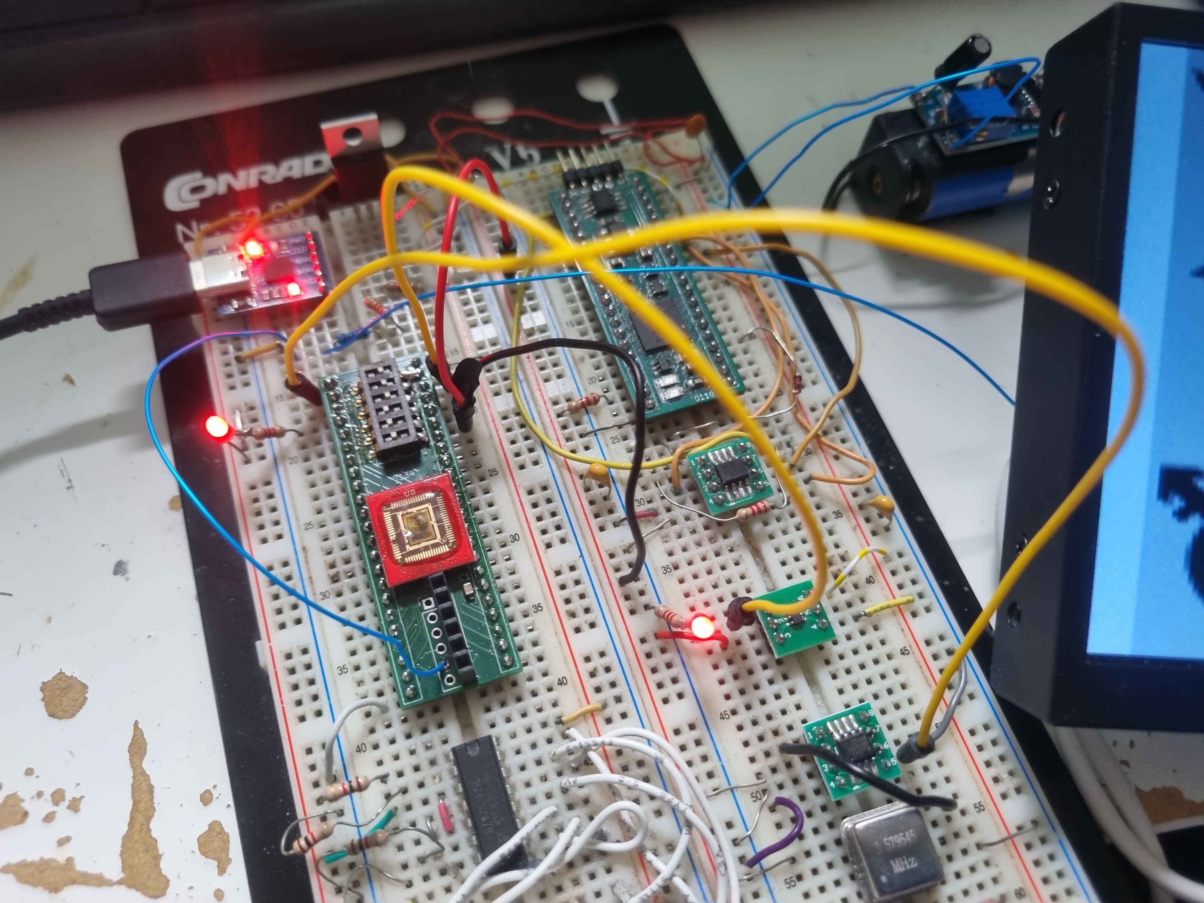
Avatar
One of the secrets on my chips that I guess I’ll reveal since I won’t be sending these hot dies to anyone anytime soon, is one of the test patterns you can get out of the NTSC video generator test. That’s why the NTSC generator macro takes up 10% of the core area. It has to encode this whole image.
💜 4
8:10 p.m.
This is the most inefficient way in which I have ever stored an image file
Avatar
And here I thought you were doing some kind of fancy subcarrier DDS math, though tbf you did mention it's not color NTSC.
Avatar
@Tholin Are you feeding them 5V or 3.3V btw ?
Avatar
18–32-gauge needles were tested.
QS815-SD https://www.indium.com/products/sintering-materials/pressureless-sintering/quicksinter/ Almost forgot some of these formulations are capable of sufficiently selective coverage to play LGA soldering.
Discover Indium Corporation's QuickSinter® sinter pastes, designed for faster sintering die-attach applications and reduced sinter time on smaller dies.
8:50 p.m.
and will bond strongly to die with Ag, Au, or Cu surfaces depending on sintering atmosphere and profile.
8:50 p.m.
Biggest issue is that top metal can't be Al.
Avatar
Avatar
Tholin
One of the secrets on my chips that I guess I’ll reveal since I won’t be sending these hot dies to anyone anytime soon, is one of the test patterns you can get out of the NTSC video generator test. That’s why the NTSC generator macro takes up 10% of the core area. It has to encode this whole image.
relatable symbols and an avali, peak test pattern
Avatar
It's a static pattern, right? I e., the signal waveform is supposed to repeat every frame?
Avatar
When PEX actually works I wanna try to throw Xyce's HB analysis at it.
9:22 p.m.
If it works at all it's going to be gloriously horrific.
9:22 p.m.
ferrisCatSneaky
9:23 p.m.
Do you use a pixel clock in there? If so, how fast or how many pixels per line?
9:29 p.m.
Hmmm, about 534 (ish) pixel "clocks" per line.... "Only" 140k (ish) harmonics of the frame (not field!) rate until hitting the luma bandwidth cap 🙁
Avatar
I’m using these numbers
9:45 p.m.
So these are the pixel clocks
Avatar
Avatar
namibj
How do you mean, "[potential for] in house bumping"? My expectation would be that if there's a way to do it wafer-scale but sufficiently selective to not be a problem for those wafer.space customers who's plans are incompatible with fcBGA (even if on a fan-out package like how the current COB is and how vaguely modern CPU/southbridge LGA/BGA packages use a high density FR4-looking PCB to fan out chip-scale bump pitch to low-cost 4-layer-desktop-mainboard compatible coarse pitch, leaving the back of the die exposed for lower-power chips that don't warrant a an indium soldered metal IHS), then some kind of bumping should be practical at cost similar to the current COB+wire-bonding, but not counting the then-necessary high-density fan-out board/interposer that would cope with the 200~300 μm ball pitch needed to match the current setup's IO count. And beyond that, I also just generally question the selection of this NIH-smelling COB "solution" vs. a classic TQFP with a vaguely-decent exposed-bottom thermal pad, overmolded in classic black filled epoxy perhaps if such available using the 150 or 175 C Tj rated epoxy they use on integrated power stages. The bonding should be same complexity as current COB bonding, and the overmolding would merely have to adjust fill volume to the 2 (technically 3) die sizes in use. Rough estimation suggests feasible R_th(junction-to-case) assuming a 5mm² hot spot zone of 0.5~1 °C/W so essentially trivial contribution and also fairly easy to cool after it's spread a bit from the copper slab it's glued to.
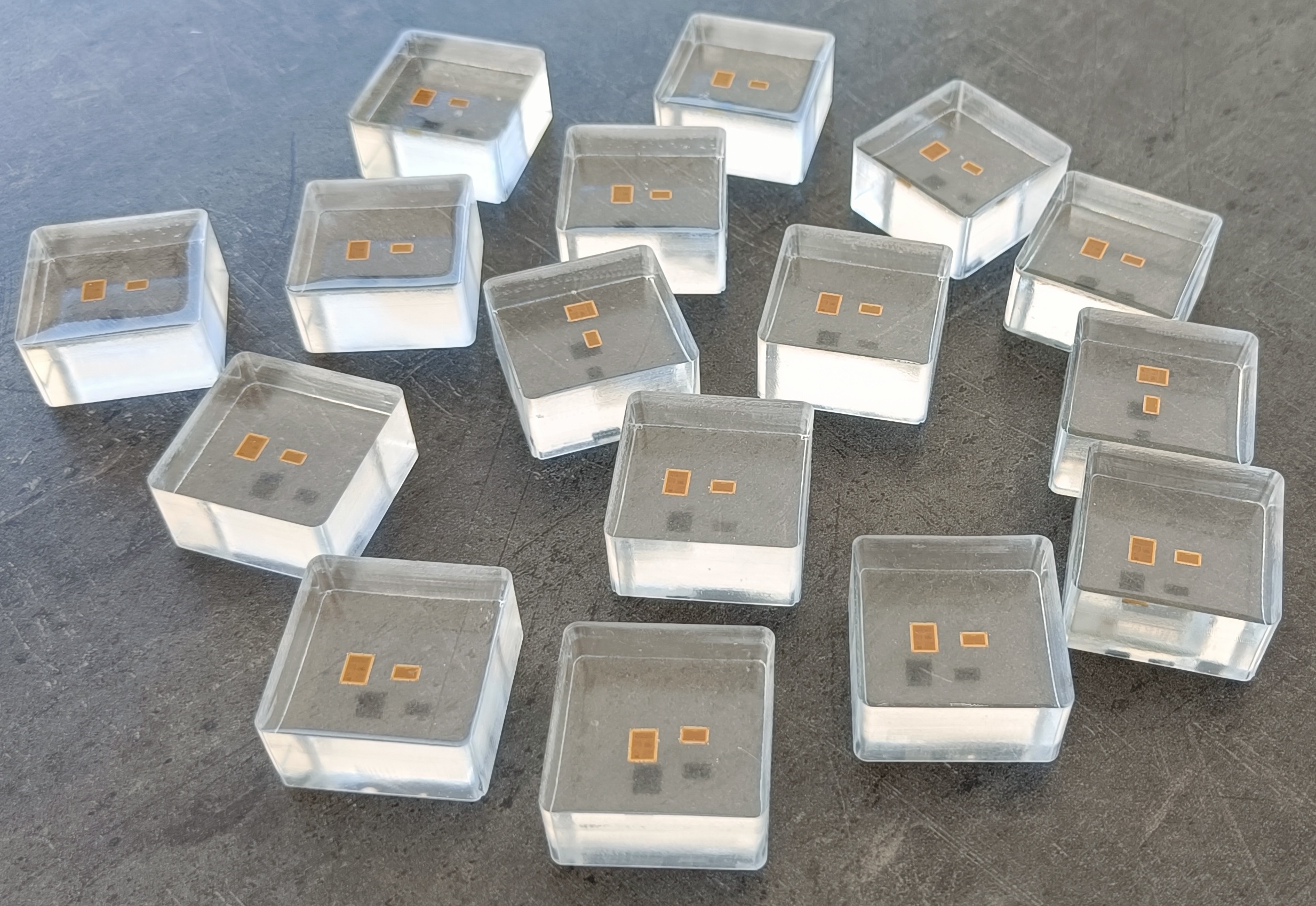
Tim 'mithro' Ansell 2026-05-22 5:50 a.m.
@namibj - If you can find a way to do TQFP for under $1.50 USD all up when doing only 1000 units, then I would be extremely happy. The cheapest I have found today ends up being ~$10 USD per chip.
Avatar
Avatar
Max Vallone
IHP published pricings in the order of 6500 eur for bumping to 18.5k eur for CU pillar. This was per MPW slot purchased however there might be potential for in house bumping and I am currently looking into testing CU or AL pillar deposition after receive run 2 GF dies. Flip chip bonding would be really nice for the higher power / density / mmIC projects my team is working on
Tim 'mithro' Ansell 2026-05-22 5:54 a.m.
iHP bumping is not compatible with something like wafer.space because they need to do it on a whole wafer and can't handle cut die. You can purchase full wafers from wafer.space (for $2k USD each) and have iHP do the bumping but you are only getting ~28 of your die per wafer -- which means you are starting at a cost of ~$70 USD per die.
Avatar
Avatar
Tim 'mithro' Ansell
iHP bumping is not compatible with something like wafer.space because they need to do it on a whole wafer and can't handle cut die. You can purchase full wafers from wafer.space (for $2k USD each) and have iHP do the bumping but you are only getting ~28 of your die per wafer -- which means you are starting at a cost of ~$70 USD per die.
My thought was to, if that's possible, do it in a way that doesn't preclude the non-bumped dies from wire bonding. Though yeah I should look more at the low temperature sintering offerings out there, I have hope some of them happens to be selective enough to work. Targeting around 0.2~0.4 mm pitch. Should only require a top metal plating at least.
Avatar
To present our students with their chips, I played around with resin for the first time. I think the resin cubes turned out quite well. Sure, there's still room for improvement, but for my first time working with resin, I think they're pretty okay. 🙂
💜 4
🧊 2
😍 1
2:11 p.m.
I think for the "display only dies", this is the ideal solution to give away or display somewhere.
Avatar
Andrew Wingate 2026-05-23 2:41 p.m.
Those look great!!
🙌 1
Avatar
Don't want to jinx it, but looks like my chip is alive! Some confusing timing issues that need to be worked out, but it appears to load and run the program 🙂
🙌 8
🎉 6
Avatar
Avatar
namibj
18–32-gauge needles were tested.
QS815-SD https://www.indium.com/products/sintering-materials/pressureless-sintering/quicksinter/ Almost forgot some of these formulations are capable of sufficiently selective coverage to play LGA soldering.
We could consider Fig.3 just with the place of which side the pillars are on switched.
4:38 p.m.
How impractical is it to coat compatible metallurgy over the native topmetal?
4:38 p.m.
(Post-dicing.)
4:41 p.m.
(They're doing 150um pitch rectangular dense grid; They mention having like 709 contacts on a test die of 11.9mm by 11.9mm.)
4:43 p.m.
MUst have had much more non-measured contacts then.....
Avatar
A full W.S slot should with that process fit up to about 768 contacts..... GLHF escaping that footprint tho, ofc.
Avatar
First go at a motherboard for TinyQV
🔥 7
💜 1
🇶 1
🇻 1
❤️ 1
RebelMike started a thread. 2026-05-25 12:52 p.m.
Avatar
Woo! Cmp, branch, alu, jmp and registers all working! (program just increments until 100 then halts). Might be time to spin a PCB for this thing. Honestly I'm pretty surprised it works 😅
🎉 7
❤️ 1
Avatar
Avatar
BreakingTaps
Don't want to jinx it, but looks like my chip is alive! Some confusing timing issues that need to be worked out, but it appears to load and run the program 🙂
Tim 'mithro' Ansell 2026-05-25 10:51 p.m.
That is super cool! I'm looking forward to seeing a video on this.
Avatar
Avatar
namibj
My thought was to, if that's possible, do it in a way that doesn't preclude the non-bumped dies from wire bonding. Though yeah I should look more at the low temperature sintering offerings out there, I have hope some of them happens to be selective enough to work. Targeting around 0.2~0.4 mm pitch. Should only require a top metal plating at least.
Tim 'mithro' Ansell 2026-05-25 10:52 p.m.
@Tim Edwards's old boss apparently has a low volume bumping process which would work for die that I'm trying to convince them to release as open source for people to use.
👀 1
Avatar
Avatar
Tim 'mithro' Ansell
@Tim Edwards's old boss apparently has a low volume bumping process which would work for die that I'm trying to convince them to release as open source for people to use.
That'd be awesome. I don't think it would even need to be that open for the first run to use it?
Avatar
Avatar
namibj
That'd be awesome. I don't think it would even need to be that open for the first run to use it?
Tim 'mithro' Ansell 2026-05-25 10:54 p.m.
If people want to be able to reproduce it at home it probably needs to be?
10:54 p.m.
FYI - I'm back in Australia now. So will have some more time to fix some #fpgas-online and a few other things.
Avatar
Avatar
Tim 'mithro' Ansell
If people want to be able to reproduce it at home it probably needs to be?
Oh well fair, it sounded like you were suggesting to use them to bump Run3/4
Avatar
My former boss. He might not appreciate being called my old boss.
😂 2
Avatar
Avatar
Tim Edwards
My former boss. He might not appreciate being called my old boss.
Vain is he?
Avatar
Avatar
Christopher
Vain is he?
Actually not at all. Purely my comment, and maybe a bit defensive, since he's only slightly older than me.
😁 1
Avatar
Avatar
Tim Edwards
My former boss. He might not appreciate being called my old boss.
Can you tell us any more about the bumping in question, like anytime you know to not be under NDA coverage? A major consideration from my pov would be "do you see any problems (not that you'll divulge any details) with using it on the same padframes that have already taped out" (see e.g. the quarter GDS I sent you for a representative tight pitch one)?
Avatar
In this work, we present flip-chip hybridisation results combining Electroless Nickel Immersion Gold (ENIG) bumping with Anisotropic Conductive Film (ACF) bonding, both developed in-house. This method enables fine-pitch interconnections without requiring wafer-level processing.
ohhhh.... https://arxiv.org/abs/2511.15562 once again, CERN engineering boundary pushing drops off technology useful beyond CERN. With aligned-particle ACF they get down to 25um pitch.
Fine-pitch hybridisation processes are essential for next-generation pixel detectors and high-density microelectronic assemblies. Conventional bump-bonding techniques, although reliable, remain costly and difficult to implement for single-die applications. In this work, we present flip-chip hybridisation results combining Electroless Nickel Im...
Avatar
Avatar
Tim Edwards
My former boss. He might not appreciate being called my old boss.
Tim 'mithro' Ansell 2026-05-26 7:01 a.m.
Fair enough 🙂
Avatar
Avatar
namibj
In this work, we present flip-chip hybridisation results combining Electroless Nickel Immersion Gold (ENIG) bumping with Anisotropic Conductive Film (ACF) bonding, both developed in-house. This method enables fine-pitch interconnections without requiring wafer-level processing.
ohhhh.... https://arxiv.org/abs/2511.15562 once again, CERN engineering boundary pushing drops off technology useful beyond CERN. With aligned-particle ACF they get down to 25um pitch.
Tim 'mithro' Ansell 2026-05-26 7:03 a.m.
There are some people who work at/with CERN lurking on this server, maybe they can make an internal enquiry about that work?
7:04 a.m.
BTW I just created the #usb channel as I'm very excited about getting some high quality USB cores going on GF180MCU.
Avatar
Tim 'mithro' Ansell 2026-05-26 8:39 a.m.
I was interested in understanding how "high" the active silicon part was in GF180MCU, so did this calculation -> https://docs.google.com/spreadsheets/d/1dc7NKRQ8zPLQ5zjTvlCQ6sERVP4lDZzYKM6wU9RbHFI/edit?gid=0#gid=0 Looks like <10um on the top of the 725um (which is back ground to ~200um) is active....
Avatar
Avatar
Tim 'mithro' Ansell
There are some people who work at/with CERN lurking on this server, maybe they can make an internal enquiry about that work?
Well, notably, they used an in-House ENIG on there-unspecified topmetal of their Timepix3 ASIC which lacked UBM; their detector ("Trench Isolated Low-Gain Avalanche Detector") already had UBM. The current 16μm spacing between the guard ring passivation opening and the bond pad passivation opening is a problem if the other side of the bonding can't make that spacing/cutoff with such precision. In theory it should be possible if the traces are all escaped inwards to the die center (at least except for GND) and then lifted up to the 2nd layer on vias, but that'd be fairly limiting in density due to via pitch vs. getting to escape straight outwards. It would be more critical to trace "wire end shape" though, as the only two critical things would otherwise have been "decently maintaining close to the nominal 50% copper/50%space dense-pitch wiring" plus "overall being to-scale within about +-0.1~0.2%" (for 1x1 slot; scales linearly with die length/width each in the same direction). The problem with having to specifically not hit the guard ring would be that the scale tolerance would now be more at the lower end of what it would have been, and further the fairly precise end of the trace that serves to form the bump would need to be located, to approximately 10% of nominal min track width/spacing aka 50% of track thickness. One good thing is that despite that, the ACF flip-chip tactic should still work if done further away from the guard ring and with e.g. via-in-pad structures from e.g. the 6L JLC special that could sustain up to 7 rows deep at 0.8 mm (cheap) to 0.6 mm (expensive) pad pitch (to escape one wire worth per layer between the non-blind via-in-pad's). Somewhere between only about 20 and 52 pads on a 1x1 slot under those limitations, though. The 7th row might also not be possible as the top layer of the PCB might need to be free of all solder mask in the entire bonding area, so it couldn't be routed between the outermost bga pads themselves as that would require them to be coated with solder mask. Though at least precise cutting of the ACF might suffice to keep the guard ring from getting bonded to: cut the ACF rectangle to stay away far enough from the guard ring so that after squishing it doesn't short the bare traces escaping outwards to the guard ring. That should thankfully be easy to cut with a fairly simple steel die cutter/stamp from a sheet of the ACF, once we'd have dialed in the correct spacing. A bit of process control via optical inspection might be needed to do that with the current guard ring to pad spacing though, to supervise the squeeze-distance and keep it "just right". An aligned stamp that doesn't pressure the guard ring area but only the pads/inner area should probably work with the thin FPC (70μm (1-layer, not the special)/110μm (2-layer, the special); but of that 25μm should be the coverlay that isn't present in the bond pad row zone). Not hard to make but probably not that cheap to adjust while dialing in...
Avatar
Avatar
namibj
Well, notably, they used an in-House ENIG on there-unspecified topmetal of their Timepix3 ASIC which lacked UBM; their detector ("Trench Isolated Low-Gain Avalanche Detector") already had UBM. The current 16μm spacing between the guard ring passivation opening and the bond pad passivation opening is a problem if the other side of the bonding can't make that spacing/cutoff with such precision. In theory it should be possible if the traces are all escaped inwards to the die center (at least except for GND) and then lifted up to the 2nd layer on vias, but that'd be fairly limiting in density due to via pitch vs. getting to escape straight outwards. It would be more critical to trace "wire end shape" though, as the only two critical things would otherwise have been "decently maintaining close to the nominal 50% copper/50%space dense-pitch wiring" plus "overall being to-scale within about +-0.1~0.2%" (for 1x1 slot; scales linearly with die length/width each in the same direction). The problem with having to specifically not hit the guard ring would be that the scale tolerance would now be more at the lower end of what it would have been, and further the fairly precise end of the trace that serves to form the bump would need to be located, to approximately 10% of nominal min track width/spacing aka 50% of track thickness. One good thing is that despite that, the ACF flip-chip tactic should still work if done further away from the guard ring and with e.g. via-in-pad structures from e.g. the 6L JLC special that could sustain up to 7 rows deep at 0.8 mm (cheap) to 0.6 mm (expensive) pad pitch (to escape one wire worth per layer between the non-blind via-in-pad's). Somewhere between only about 20 and 52 pads on a 1x1 slot under those limitations, though. The 7th row might also not be possible as the top layer of the PCB might need to be free of all solder mask in the entire bonding area, so it couldn't be routed between the outermost bga pads themselves as that would require them to be coated with solder mask. Though at least precise cutting of the ACF might suffice to keep the guard ring from getting bonded to: cut the ACF rectangle to stay away far enough from the guard ring so that after squishing it doesn't short the bare traces escaping outwards to the guard ring. That should thankfully be easy to cut with a fairly simple steel die cutter/stamp from a sheet of the ACF, once we'd have dialed in the correct spacing. A bit of process control via optical inspection might be needed to do that with the current guard ring to pad spacing though, to supervise the squeeze-distance and keep it "just right". An aligned stamp that doesn't pressure the guard ring area but only the pads/inner area should probably work with the thin FPC (70μm (1-layer, not the special)/110μm (2-layer, the special); but of that 25μm should be the coverlay that isn't present in the bond pad row zone). Not hard to make but probably not that cheap to adjust while dialing in...
Tim 'mithro' Ansell 2026-05-26 8:55 a.m.
I think I somewhat understand what you are saying here, but only barely...... While in Shenzhen I did make some contacts with groups who do "chip on glass" and "chip on film" stuff and are open to doing some experiments.
Avatar
Avatar
Tim 'mithro' Ansell
I think I somewhat understand what you are saying here, but only barely...... While in Shenzhen I did make some contacts with groups who do "chip on glass" and "chip on film" stuff and are open to doing some experiments.
Great. If we manage to "easily" do post-dicing ENIG bumping on the gf180mcuD dies then it'd at worst be a question of possibly increasing pad pitch though, I'm sure. And probably you convincing glofo to not whine about a passivated guard ring to us. Bonus would be that to my understanding the result would be at least gold wire bond compatible and should also be directly solder-compatible, though, so starting about Run5 it could be considered to be done pre-dicing.
Avatar
Tim 'mithro' Ansell 2026-05-26 9:10 a.m.
Probably stupid question -- but is there a simple way to coat just the exposed metal area without coating the SiN?
Avatar
Avatar
Tim 'mithro' Ansell
Probably stupid question -- but is there a simple way to coat just the exposed metal area without coating the SiN?
Yeah ENIG
9:11 a.m.
Basically just do the stuff that they do to PCBs.
Avatar
Tim 'mithro' Ansell 2026-05-26 9:12 a.m.
Like it feels like just dipping the chip into molten metal bath would cause only the exposed metal areas to get a coating?
Avatar
And destroy the chip ?
9:15 a.m.
You pretty much can't "solder" to Al hence why ENIG. Electro-less desposition of nickel alloy and then some gold over tha. To make a surface that will "wet" to solder AFAIU.
Avatar
Avatar
tnt
You pretty much can't "solder" to Al hence why ENIG. Electro-less desposition of nickel alloy and then some gold over tha. To make a surface that will "wet" to solder AFAIU.
Tim 'mithro' Ansell 2026-05-26 9:18 a.m.
If I understand correctly, you can't "solder" to Al due to the Al oxide layer which quickly forms when pure Al is exposed to air. The wire bonding process using Al uses one of a number of methods to "punch through" the oxide layer and weld the Al wire to the metal.
9:23 a.m.
Interestingly was just trying to figure out how ENIG process actually works and found the following
Avatar
It apparently needs a zinc[ate] base layer if done on Aluminum though to chemically alloy through the natural oxide of the Aluminum; I don't think that's a problem though. It would require the guard ring to not be exposed top metal, though! And it's much more involved than "just" taking JLC-special FPC (25μm polyimide core with 13μm copper either side and 50.8μm minimum trace width/spacing (76.2μm "recommended" but for this task of escaping the bond pads straight out and fanning to the +50% wider pitch starting after about 200~500μm beyond the nominal bond pad border, the 50.8μm DRC minimum shouldn't cause a yield too low to just eat and given that FPC-to-die alignment would AFAIK practically have to be done optically through the orange (but otherwise clear see-through) tint of the polyimide, I'd expect AOI of the entire FPC area that's below recommended DRC minimums to be practical and easy at least if we'd not obscure that area with the non-die-facing copper layer. In that case we'd probably want/have to "instead" go for a dedicated AOI screening of the chip-facing area from that side before flipping it and aligning it to the die's pads and then locking in the alignment with the cold mild pressure tacky aspect of the ACF before perhaps doing one more AOI check to confirm tacking didn't shift it, before then releasing it to the hot stamp that applies that 2MPa from the top through a heated pad with the die probably resting against an anvil during it.
Avatar
Avatar
tnt
You pretty much can't "solder" to Al hence why ENIG. Electro-less desposition of nickel alloy and then some gold over tha. To make a surface that will "wet" to solder AFAIU.
You can solder Al but the reason to not hot dip plate it is for precision mostly, as it's fairly hard to control thickness with hot dip. Besides of course temperature resistance severely limiting metal choices.
Avatar
Tim 'mithro' Ansell 2026-05-26 9:30 a.m.
@namibj - As I said, in Shenzhen I met a few groups that do FPC related stuff. If I can figure out how to communicate things we could probably try it......
Avatar
Avatar
Tim 'mithro' Ansell
Interestingly was just trying to figure out how ENIG process actually works and found the following
Electroless nickel plating. https://en.wikipedia.org/wiki/Electroless_nickel-phosphorus_plating See https://www.protoexpress.com/kb/enig/ for the standard ENIG, https://www.protoexpress.com/kb/enepig-surface-finish/ for a variant that's still very wire-bondable ("It is ideal for solder joint strength, aluminum wire bonding, and gold wire bonding."), and https://www.protoexpress.com/kb/epig-surface-finish/ for if one has complaints about the minimum thickness of the plating when it's used on e.g. a PCB in a BGA fan-out with needs for severely small trace width (these processes are fairly isotropic so the plating thickness will also build up sideways; while the initial copper trace width minimums are mostly given by the trace itself becoming unstable to litho if too narrow, and rings around via holes risking becoming cut by the drill which thus clearly won't just grow back as part of the plating once it's gone).
Electroless nickel-phosphorus plating, also referred to as E-nickel, is a chemical process that deposits an even layer of nickel-phosphorus alloy on the surface of a solid substrate, like metal or plastic. The process involves dipping the substrate in a water solution containing nickel salt and a phosphorus-containing reducing agent, usually a h...
ENIG (Electroless nickel immersion gold) is a two-layer metallic surface finish that includes a thin layer of gold over a layer of nickel.
ENEPIG is the most used lead-free surface finish. It influences assembly capability, PCB shelf life, solder joint quality, cost, and performance.
EPIG is a lead-free, RoHS-compliant, and noble-metal-based PCB surface finish that protects copper from oxidation.
Avatar
Avatar
Tim 'mithro' Ansell
@namibj - As I said, in Shenzhen I met a few groups that do FPC related stuff. If I can figure out how to communicate things we could probably try it......
Yeah just be up-front about us having pre-diced Aluminum-Topmetal dies with SiN passivation, these 60μm (standard and we have dies) square passivation openings, with 102μm ("vertical")/104μm ("horizontal") pad pitch and apparently a 16μm span covered by SiN before the guard sing comes, who's SiN opening is apparently 9μm wide. That's for the quarter-slot TinyQV dies of Run1; I don't think there's reasonable need to go for any denser pitch in a 1-row-deep padring layout even for the larger dies. E.g. @Tholin's die (1x1 slot, Run1; tho I had to build the GDS myself and had to [turn off the custom images as I couldn't easily figure out how they are to be built (like, what parameters I'm supposed to use to get the same pixels-to-gds processing done as was done for the Run1 tapeout), and there's some hidden-secret-code (like, a capture-the-flag thing or such?) hard-macro to be synthesized from redacted verilog (didn't build as it's in the repo! Had to get AI to cook that redacted verilog to get something that'd build (and should at least play nice with the rest of the die without me having to touch the multiplexer and any more global PnR beyond unleashing the former image zones for global PnR...) 🙁 )...] ) has same pad size and spacing to guard ring, but 211μm ("vertical")/180μm ("horizontal") pad-pitch instead. I'm mostly mentioning that one because it's looking to particularly expect to benefit from getting a flip-chip mounting applied to (some of) the remaining dies to thus enable some good back-side cooling.


Avatar
Avatar
Tim 'mithro' Ansell
Like it feels like just dipping the chip into molten metal bath would cause only the exposed metal areas to get a coating?
In practice you'd do a (usually water-based) catalytic or redox/displacement plating solution [using a more noble metal's dissolved salt to sacrifice the thin surface layer of the mostly-not-oxidized (that's a minor complication with Aluminum sadly) base metal to essentially locally at molecular scale create shorted-out "batteries" that "discharge" into creating the desired layer of the more-noble metal over the base as thick as this molecular-scale process can penetrate into the base metal; the consumed base metal ends up as the salt in the solution. Yes, if you do that with mixed solid power of "noble metal salt" and "less-noble mostly-bare metal" and use high heat to just about melt them together, the very same reaction is called "thermite".] at/near room temperature.
Avatar
Tim 'mithro' Ansell 2026-05-27 12:17 a.m.
@namibj - So what actually would be the next steps that make sense?
Avatar
I'd see if at least something big enough to test bond pad pitch on can get into Run2 with a passivated seal ring; I'd see about spin coating for shed litho passivation onto that currently (Run1 dies) exposed metal seal ring, and find someone who'd dip 3~5 dies through al-plating electroless baths starting with the zincate that seems to be needed to tame the aluminium oxide. Then if that's found, I'd get JLC to make me a 2$ special: 5pcs 100x100mm FPC, 2L, ENIG, 1/3oz (12um) copper each of the two layers, and spend 20 min looking for a better choice than the ACF that @BreakingTaps had used, if not finding anything better in that time, going and just ordering a roll of that that will live in the freezer in a suitable resealable moisture barrier metallzied foil bag if I have one, or just how it came in a freezer bag if I can't find a resealable metallized one. I'd find me a microscope and for a first probably just try to boond two of the FPCs to each other with the proper alignment, either doing end-result-focused process control for thermals, or calibrating with a thermocupuple dymmy of suitable thickness, with pressure calculated based on contact area and if I'd have my hands on any, quite possibly using a decent CNC axis to apply the presure through a couple millimeters of spring travel to make the entire hot-clamp more compliant. If I'd have access to one that's made for this hot ACF bonding, I'd see to just use that instead of hacking a hot stamp that can apply dialed-in pressure/force and releases after an electronic timer.
12:32 a.m.
I don't know why they are so intense about exposing the seal ring top metal unless it's an official flip chip die.
12:34 a.m.
it would be really good if you could find out if we can get rid of that without cannibalizing more important DRC/process custom treatment quota.
Avatar
Tim 'mithro' Ansell 2026-05-27 8:05 p.m.
@namibj - Is there anything we can do with the current die and their 40um x 40um openings?
Avatar
Avatar
Tim 'mithro' Ansell
@namibj - Is there anything we can do with the current die and their 40um x 40um openings?
If we can passivate the adjacent guard ring strong enough to resist the ACF's nickel spheres, it should be straight forward to bond with 10$ of parts (a roll of ACF and a JLC special FPC) and access to a device that can do the heated pressing, which would give 5 dies and most of the ACF left over. Ideally we'd passivate the ring and then do a standard zincate-base ENIG and then the ACF or even try to directly LGA solder (use something that is thermal expansion matched to the silicon or so weak/thin the silicon isn't stressed too much). I suggest asking one of the people around who have done some diy litho how easy it'd be to litho a passivation layer on the outside border beyond the pads to cover the guard ring; it's nominally 16μm gap in which the line/edge of the sheet should land. I'd try spin coating some clear UV nail polish (aka UV activated acrylic resin in small cheap bottles) or resin 3d printer resin, and either place a simple metal foil sheet over the area with the pads to shield them from the coming light, or mount a blu ray laser diode with the optics to something that let's us draw along the guard ring without (substantial) hitting the pads; then using a weak solvent to wash it off before applying the ACF. Or find a way to stick some thin (about 5~30μm) tape on the edge without obstruction the pads, then apply ACF.
8:29 p.m.
In acute cases of flip chip need, ball wire bonding can be used to form studs on the pads; it is my understanding that the result is suitable for at least some types of flip-chip bonding acting as a replacement for wafer bumping. I don't think that's an effective way forward that could beat the current COB pricing for a Run4/5, though. I'd expect it to be around twice as expensive as the current bonding, not speaking of the ease of finding a bone house that can do it economically at the volumes.
Avatar
Tim 'mithro' Ansell 2026-05-27 8:38 p.m.
Wouldn't the guard ring be under the passivation?
Avatar
Avatar
Tim 'mithro' Ansell
Wouldn't the guard ring be under the passivation?
Well I thought so but apparently the DRCs say that it is under passivation if and only if you select "flip chip" for the flavor of DRC deck. I do not know why they consider it mandatory to expose it when not doing flip-chip, instead of just recommending. I have confirmed that the PAD layer in the GDS is drawn over the ring on several of the Run1 chips; you're in a position to see if any of them don't have it drawn over that ring. And to see or if needed ask whether they care about it being hidden (under passivation) for dies that get partial flip-chp treatment. This might not be a rule that is enforced at your submission stage, but just from the openPDK when trying to submit into your MPW.
Avatar
Avatar
namibj
Well I thought so but apparently the DRCs say that it is under passivation if and only if you select "flip chip" for the flavor of DRC deck. I do not know why they consider it mandatory to expose it when not doing flip-chip, instead of just recommending. I have confirmed that the PAD layer in the GDS is drawn over the ring on several of the Run1 chips; you're in a position to see if any of them don't have it drawn over that ring. And to see or if needed ask whether they care about it being hidden (under passivation) for dies that get partial flip-chp treatment. This might not be a rule that is enforced at your submission stage, but just from the openPDK when trying to submit into your MPW.
Tim 'mithro' Ansell 2026-05-27 9:47 p.m.
Also, why does it matter if the guard ring was connected?
Avatar
Avatar
Tim 'mithro' Ansell
Also, why does it matter if the guard ring was connected?
because it would short to every trace of the FPC; the FPC's solder mask is far far far from supporting being present on the 16um away guard ring exposed metal but having the metal of the IO pad nice and exposed for the ACF to contact. Also it's not that thin, but that's a lesser problem to that. What should work actually now that I think about it is taking an FPC but fan out to the middle, glueing that FPC with soluble glue (e.g. PVA glue dissolved with water) to a stiff carrier, then carefully sanding down the edges until they no longer reach over the pads to the guard ring. I'd suggest a 1x1 slot and going for an easy to solder SMD connector placed in the middle; I don't think the current mezzazone connector is necessarily short enough to fit though. It might diagonally fit well enough? But there would be little room to route. The connector would be soldered after the ACF is hot pressed. The FPC would be optically aligned to the pads on grounds of being kinda see-through just orange-tinted, then lightly pressed down onto the ACF to use it's natural slight tackyness to transport it to the hot press equipment. I'd assume that the temperature and pressure are mildly sensitive but the time could be exceeded upwards fairly low-risk as far as yield goes, so a heavy thing on a lever arm (to keep it from putting uneven pressure on the die) pressing down through the recommended feflon foil over 0.2~0.3 mm of shore70+ silicone (onto the FPC; the die would be on a hard surface below), with one of the two sides being heated to the recommended 18~190C, should give functional results with ingredients on the level of "cabinet hinge"+"2by4"+"soldering hotplate that doesn't get crushed"+"gallon jug (adjustable with water)" to rig a 2 MPa-ish repeatable press.
10:02 p.m.
It's just that the escape to the inside style doesn't allow for increasing the IO to similar pad spacing as we have on the quarter tile, which would be the case for the escape outwards that needs the guard ring not shorting out all the bonds.
10:09 p.m.
the concept approximately for the escape-outwards is a "leadframe"-like structure litho'd onto the polyimide base of the FPC (just a regular FPC manufacturing), which is then flip-chip bonded to the pads of the die. But as far as the die can tell, those copper traces are fully exposed towards the die. The polyimide is just on the back to keep them from moving and to provide further mechanical support and to allow it to be manufactured. Outside the die area it can then also cover up with the coperlay the traces, but that's not practical right at the pads. This wouldn't be so hard if the guard ring was more than those 16um away from the pad edge. The coverlay would need about 150~250um gap to handle it well.
Avatar
Tim 'mithro' Ansell 2026-05-28 1:00 a.m.
@namibj - I think I understand the issue with the guard ring now, it is very close to the pads and whatever is trying to bond to pads is likely to accidentally connect with the guard ring and the guard ring would short everything together.
1:01 a.m.
@Leo Moser (mole99) - are you able to confirm that there is no polyimide/oxide over the top of the guard ring structure?
Avatar
Avatar
Tim 'mithro' Ansell
@Leo Moser (mole99) - are you able to confirm that there is no polyimide/oxide over the top of the guard ring structure?
Notably it should look like pad not like PDN if I'm right.
Avatar
Avatar
Tim 'mithro' Ansell
@namibj - I think I understand the issue with the guard ring now, it is very close to the pads and whatever is trying to bond to pads is likely to accidentally connect with the guard ring and the guard ring would short everything together.
Also it's much closer than the gap between pads (~3x) and right in the way of where one would want the lead frame traces to go from the pads. Without that you could take a PCB footprint like the wirebond fan out just all the way to the pads, flip the chip, put ACF between, and in theory a clothes iron set zu 2.5 for about 3 to 15 seconds. In practice one wants a bit more precision in control to maintain good yield without dies delaminating from the board due to poorly hardened epoxy nor poor electrical contract/occasional shorts between adjacent pads. Also JLC AFAIK only sells that very fine pitch (102μm used on quarter slot) on 1/3oz FPC. But benefit, both FPC and ACF are see-through so no dedicated fiducials would be required.
Avatar
Avatar
Tim 'mithro' Ansell
@Leo Moser (mole99) - are you able to confirm that there is no polyimide/oxide over the top of the guard ring structure?
Leo Moser (mole99) 2026-05-28 6:25 a.m.
Yes, there is a 9um wide glass cut in the seal ring/guard ring structure. Likely to prevent cracking during dicing. However, the guard ring for flip-chip packaging has no glass cut:
to be protected from chemical attack during solder bumping process.
You can find both layouts here: https://gf180mcu-pdk.readthedocs.io/en/latest/physical_verification/design_manual/drm_12_2.html
Avatar
Interesting the DRM also says the guard ring should be directly connected to VSS pads. Not sure we do that.
Avatar
Avatar
tnt
Interesting the DRM also says the guard ring should be directly connected to VSS pads. Not sure we do that.
Leo Moser (mole99) 2026-05-28 6:56 a.m.
No, we currently don't do that. I assume they the guard ring should be grounded due to ESD reasons? We could connect the VSS pads on the other side directly to the guard ring. However, KLayout DRC would throw an error since unrelated Nwell, COMP, Poly2, Metal must be 10um away. Not sure how they implemented that exception.
6:57 a.m.
The other question is how to implement that in the template in an automated manner.
Avatar
Avatar
Leo Moser (mole99)
Yes, there is a 9um wide glass cut in the seal ring/guard ring structure. Likely to prevent cracking during dicing. However, the guard ring for flip-chip packaging has no glass cut:
to be protected from chemical attack during solder bumping process.
You can find both layouts here: https://gf180mcu-pdk.readthedocs.io/en/latest/physical_verification/design_manual/drm_12_2.html
The DRC there claim it's mandatory to expose on non-flipchip and forbidden to expose on flipchip. I understand yield impact potential, but exposing the metal is as explained quite in the way of even trailing non-wire-bonded packaging approaches.
Avatar
Avatar
Leo Moser (mole99)
No, we currently don't do that. I assume they the guard ring should be grounded due to ESD reasons? We could connect the VSS pads on the other side directly to the guard ring. However, KLayout DRC would throw an error since unrelated Nwell, COMP, Poly2, Metal must be 10um away. Not sure how they implemented that exception.
Also they say guard ring can be used for down-bonding if it's a little widened.
Avatar
Avatar
Leo Moser (mole99)
The other question is how to implement that in the template in an automated manner.
VSS pad comes with the bridge to the ring.
6:13 a.m.
(would be my suggestion for how-to)
Avatar
Avatar
namibj
The DRC there claim it's mandatory to expose on non-flipchip and forbidden to expose on flipchip. I understand yield impact potential, but exposing the metal is as explained quite in the way of even trailing non-wire-bonded packaging approaches.
Tim 'mithro' Ansell 2026-05-29 6:46 a.m.
Maybe having a break in the top silicon oxide might prevent cracks from propagating / running?
Avatar
Avatar
Tim 'mithro' Ansell
Maybe having a break in the top silicon oxide might prevent cracks from propagating / running?
Leo Moser (mole99) 2026-05-29 6:49 a.m.
Yes, that's what I was suggesting :)
Avatar
Avatar
namibj
VSS pad comes with the bridge to the ring.
Leo Moser (mole99) 2026-05-29 6:50 a.m.
Yeah, that would work for the implementation. However, the DRC deck would also need to be updated, as it ensures that there are no shapes within 10 µm of the guard ring.
Avatar
Avatar
Tim 'mithro' Ansell
Maybe having a break in the top silicon oxide might prevent cracks from propagating / running?
It's nitride, and fair, but (a) do we know the yield impact, and (b) would glofo get annoyed if we include one die without that exposed top metal on the guard ring in Run2?
Avatar
The amount of pings and DMs I’ve gotten about my SCL over the past week is crazy
6:16 p.m.
Are people actually using it?
Avatar
what's SCL?
Avatar
Standard Cell Library
Avatar
Avatar
Tholin
Are people actually using it?
I've been using it
Avatar
Avatar
Tholin
Are people actually using it?
@tnt suggested me to go for it for the 32 bit per clock PRBS-31 generator (and indirectly some misc config bits of sort that'll have to find a place to live), for the MCML VCO + Gigabit-TX-only-"transceiver"I failed to get finished for ttsky26a and have now chosen the opportunity of ttgf0p3 to (hopefully) tape out in W.S. Run2 instead.
Avatar
I’m using it - idea is to see if we can prove your library + the 3v3 SRAMs all work together in TinyQV on run 2.
Avatar
And I need to do MCML<->SCL level shifters, for: 1. Feeding SCL-sourced 16/32 wide bitstream to MCML MUX stages. 2. Clocking the bitstream feed from the (appropriately divided) VCO. (edited)
Avatar
Tim 'mithro' Ansell 2026-05-30 12:04 a.m.
❤️ 3
12:04 a.m.
This is so cool!
❤️ 1
12:06 a.m.
Avatar
asic destroyer 2026-05-30 9:40 a.m.
I've also provided ready-to-use images that can boot Zephyr RTOS and MicroPython .
Avatar
Avatar
Tim 'mithro' Ansell
@namibj - I think I understand the issue with the guard ring now, it is very close to the pads and whatever is trying to bond to pads is likely to accidentally connect with the guard ring and the guard ring would short everything together.
If you don't have to use that area for other structures, I'd suggest we put some flip chip bond test structures in the side strip of the reticle, as those are too small to really use with any normal padframe and look to be mostly barren in the stretched tape wafer pictures from today?
Exported 689 message(s)
Timezone: UTC+0